

This article presents energy-efficient quaternary minimum and maximum logic circuits based on carbon nanotube field-effect transistor (CNTFET). The specific features of CNTFET, such as the possibility of determining the desired threshold voltages which are obtained by acquiring suitable diameters for carbon nanotubes, facilitate designing efficient circuits with multiple threshold voltages. The proposed minimum and maximum circuits are designed using an efficient combination of quaternary multiplexers and specific ternary buffers. The proposed designs are simulated using Synopsys HSPICE with the Stanford 32nm CNTFET technology and the performance parameters and sensitivity to process and temperature variations are evaluated through comprehensive simulations. The results demonstrate that the proposed QMin and QMax designs operate with high robustness even in the presence of major process variations. In addition, they have 51% and 63% lower power-delay product (PDP) and 64% and 61% lower energy-delay product (EDP), respectively, as compared to the state-of-the-art CNTFET-based quaternary circuits recently presented in the literature.
In recent years, nanoscale CMOSes have encountered some challenges with respect to design and manufacturing such as increased leakage currents, decreased gate control and degraded I–V characteristics. Modern nanotechnologies have been introduced for implementing nanoscale circuits such as quantum-dot cellular automata (QCA), single electron transistor (SET), and carbon nanotube field effect transistor (CNTFET) to resolve such challenges. Low power consumption, ballistic transport under low supply voltage, and small dimensions are among the features of such nano-devices for designing ultra-low-power and ultra-high-density integrated circuits (Abu El-Seoud, El-Banna, & Hakim, 2007; Keshavarzian & Navi, 2009; Keshavarzian & Sarikhani, 2013; Raychowdhury & Roy, 2005; Tehrani, Safaei, Moaiyeri, & Navi, 2011). Meanwhile, CNTFET can be considered as the best alternative for MOSFET-based circuits as it has higher resemblance with MOSFET and offers a high current gain (Moaiyeri, Faghih Mirzaee, Navi, & Momeni, 2012a).
Multiple-valued logic (MVL) circuits have gained more attention in CNTFET technology during the recent years as they are suitable devices for designing MVL circuits with multiple threshold voltages. Multiple threshold voltages can be provided by adopting the required diameters for the nanotubes of a CNTFET (Lin, Kim, & Lombard, 2012).
The recent VLSI chips are faced with difficulties in placement and routing of the logic blocks and very large area of interconnects. Moreover, the pin-out constraint limits the number of connections of an integrated circuit with the external world and makes the packaging process more complicated. In addition, implementing many complex applications such as process control and decision systems is usually useless and impractical in binary logic.
In order to resolve these problems, digital systems using radices greater than two and multiple-valued logic (MVL) circuits should be taken into account. MVL systems work with more than two allowed logics. It is worth noting that the four-level logic (quaternary logic) benefits from ease of conversion between quaternary signals and binary signals which are produced by the existing binary circuits.
By utilizing MVL instead of binary logic the data content per interconnection is increased which reduces the number of wires. Also, pins of chips carry more information which decreases the number of required pins. In addition, MVL provides considerably more information compaction on logic circuits which has been successfully carried out in very dense flash memories, where a single memory cell can hold numerous logic values.
In arithmetic circuits, redundant number systems can reduce or even omit the rippling carries that leads to faster arithmetic operations as compared to the normal binary logic. Moreover, MVL can be even applied to solve the binary problems more effectively. For instance, a third logic value can be utilized as a medium for signaling the faulty operation in testing the binary circuits (Moaiyeri, Navi, & Hashemipour, 2012b).
Different methods for designing MVL circuits have been presented so far in the literature. However, most of them suffer from some critical drawbacks. For instance, the designs of (Mouftah & Jordan, 1974; Mouftah & Smith, 1982; Raychowdhury & Roy, 2005) need very large resistors. The CNTFET-based quaternary logic gates presented in (Moaiyeri et al., 2012b) function based on resistive voltage division at the output CNTFET stage which considerably increases the power consumption. However, the output drivers of these circuits enhance their drivability and considerably reduce the propagation delay. Efficient multiple-valued logic gates have been presented in (Liang, Chen, Han, & Lombardi, 2014) based on the pseudo n-type method which reduces the design complexity. However, the ratioed logic of the pseudo n-type method leads to higher propagation delay and power consumption and consequently less energy efficiency. In addition, it reduces the output logic swing that also increases the delay and static power consumption and degrades the robustness when these gates drive next stages. Moreover, in general, each quaternary function can be implemented using quaternary multiplexers (Datla, 2009). However, purely multiplexer-based design does not result in a hardware-efficient circuit.
In this paper, robust and energy-efficient CNTFET-based quaternary minimum and maximum circuits are designed for nanoelectronics based on an innovative combination of quaternary multiplexer, threshold detectors and specific ternary buffers.
In the remainder of the paper, in Section 2 the CNTFET device is briefly reviewed. In Section 3 the proposed designs are presented. The simulation results are represented in Section 4 and finally Section 5 concludes the paper.
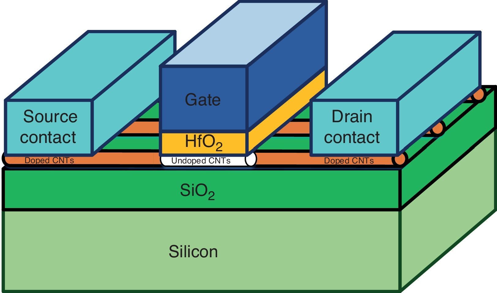
2Carbon nanotube field effect transistor (CNTFET)Carbon nanotubes (CNTs) are graphite cylindrical sheets, which are categorized into two groups: single-walled carbon nanotubes (SWCNTs) that are made of a cylinder; and multi-walled carbon nanotubes (MWCNTs) that are made of more than a cylinder (McEuen, Fuhrer, & Park, 2002). There is a chirality vector for any carbon nanotube, which is specified by a pair (n, m) and determines the angle of carbon atom formation along the nanotube. Specifications of nanotubes depend on their structure and they can act as metal or semiconductor depending on the chirality. If (K∈ℤ) n−m≠3K, the SWCNT is semiconductor and otherwise, the SWCNT is metal. SWCNTs are used instead of silicon bulk in the channel of transistors as the channel substance of CNTFET devices, which reduces and sometimes removes many undesired parasitic elements. Electrons and holes do not have an identical mobility in silicon whereas n-type and p-type CNTFETs have similar mobility (μN=μp). This feature of CNTFETs facilitates the transistor sizing, as the complexities will be fewer than the ones of MOSFET-based design. CNTFET nanodevice has similar I–V characteristics as compared with a well-tempered MOSFET, which is another advantage of CNTFETs (Moaiyeri, Doostaregan, & Navi, 2011).
CNTFETs have three types including Schottky barrier CNTFET (SB-CNTFET), tunneling CNTFET (T-CNTFET) and MOSFET-like-CNTFET (Raychowdhury & Roy, 2007). However, the MOSFET-like CNTFET is more suitable for designing circuits based on the CMOS style because of their inherent electrical characteristics and transistor structure. Another feature of the MOSFET-like CNTFET is that drain/source-channel connections have no Schottky barrier and it has a considerably higher ON current. Figure 1 shows a MOSFET-like CNTFET structure.

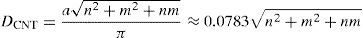
According to Figure 1, the distance between the centers of two adjacent nanotubes is called pitch, which has a direct impact on the width of the connections and gate of the transistor. The width of the gate of a CNTFET is estimated by the following equation (Kim, Kim, & Lombardi, 2009):
where N is the number of nanotubes under the gate, Wmin is the minimum width of the gate determined by the photolithography process and DCNT is the diameter of carbon nanotube, which is calculated as given in Eq. (2), where, a≈0.249nm is the lattice constant in a CNT structure (Kim et al., 2009):
The threshold voltage (Vth) of a CNTFET can be determined by adopting proper CNT diameters, which is obtained from Eq. (3) (Kim et al., 2009):
where e is the unit electron charge, Eg is the CNT band gap, Eπ (≈3.033eV) is the energy bond of carbon π–π in the tight bonding model.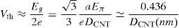
Many feasible and effective approaches have already been presented in the literature for growing CNTs with a specified chirality and determining the desired threshold voltage for multi-tube CNTFETs (Lin et al., 2009; Yang et al., 2014). Nevertheless, designing CNTFET-based circuits with fewer number of required CNT reduces fabrication costs and enhance the manufacturability.
3The proposed quaternary circuitsAs minimum (logical multi-valued AND) and max (logical multi-valued OR) operators are the most fundamental blocks of multiple valued logic systems, an appropriate design of these two operators can be effective in enhancing the performance and energy-efficiency of MVL systems. In this paper a new method for designing energy-efficient quaternary logic circuits is proposed.
The proposed method utilizes a quaternary 4-to-1 multiplexer (QMux) consisting of a selector (generated by a quaternary decoder) and a quaternary transmission gate network (QTG) and also threshold detector (TD) circuits. An efficient design for CNTFET-based quaternary multiplexer has been presented in (Moaiyeri et al., 2012b), which is shown in Figure 2.
. (a) Quaternary decoder. (b) TG network.")
CNTFET-based quaternary Mux (Moaiyeri, Navi, et al., 2012). (a) Quaternary decoder. (b) TG network.
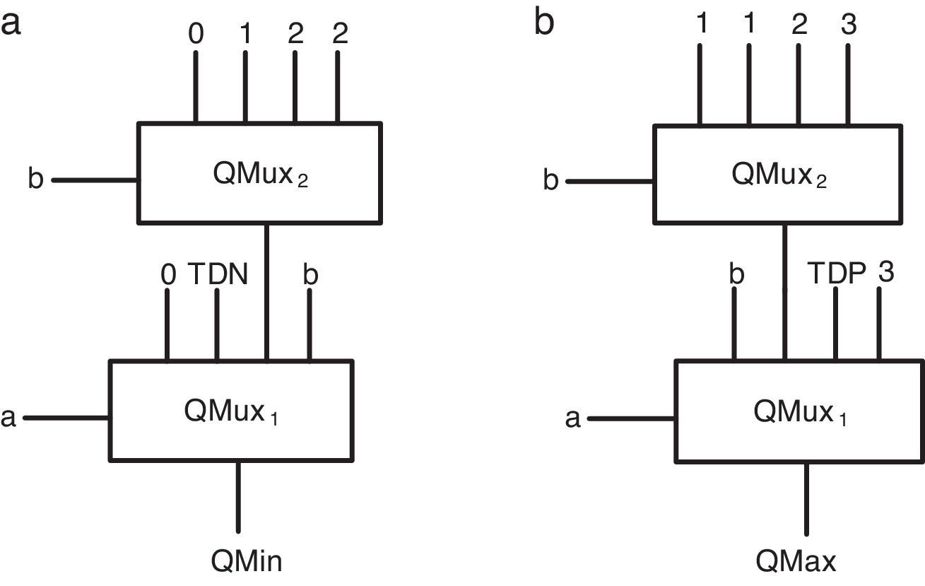
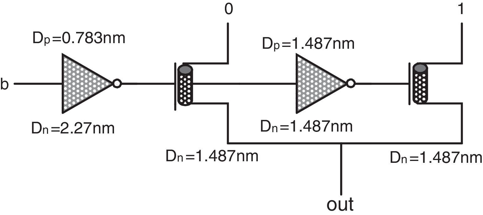
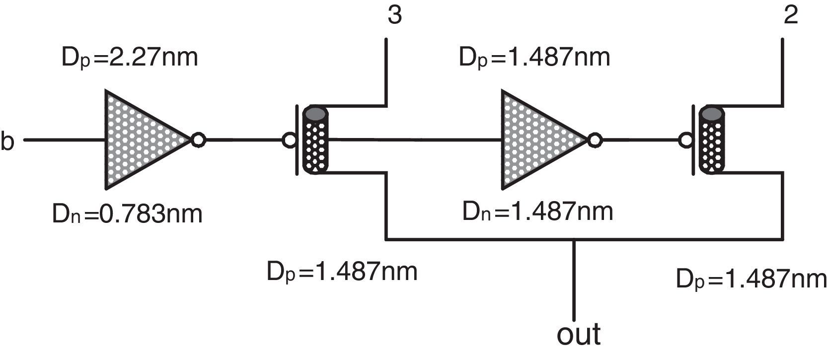
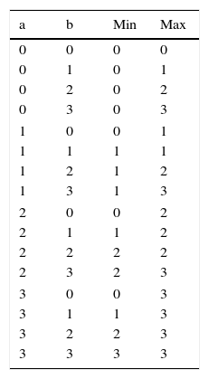
Figure 3(a) and (b) show the basic schema of the proposed quaternary minimum and maximum circuits, respectively. In these two circuits, the QMux shown in Figure 2 is used as the main body of the circuit. The four inputs of the QMux circuits are assigned as per Table 1, and accordingly the output of QMux1 will be the quaternary minimum signal (QMin) or the quaternary maximum signal (QMax).
 Quaternary min. (b) Quaternary max.")
As Table 1 shows, input a can be used as a selector in QMux1. Therefore, it is possible to divide the table into 4 sections based on different logic levels of a and adjust each input of QMux1 for each section of the table. To adjust QMux1 input pins in QMin circuit, we act as follows:
In the first section (a=0), the QMin output has always a zero logic. Therefore, it is possible to connect the first QMux1 pin to zero logic without using any intermediate.
In the second section (a=1), the QMin output has 0 and 1 logics. According to the table, if b=0, QMin equals 0. Otherwise (b≠0), QMin equals to 1. Therefore, an nMOS-based threshold detector (TDN) module can be used, which is switched on logical ‘0.5’ and is controlled by the input signal b through the inverters (Moaiyeri et al., 2012b). Figure 4 shows the nMOS-based TD circuit.
.")
In the third section (a=2), QMin output has 0, 1, 2 and 2 logics, respectively. In order to realize these logics in the third QMux1 input pin, another multiplexer (QMux2) with input selector b can be used. Accordingly, the inputs of QMux2 should be connected to 0, 1, 2, 2 logics.
In the fourth section (a=3), the QMin output is similar to input b. Therefore, it is possible to connect the fourth QMux1 input pin to the input b without using any intermediate.
To adjust QMux1 input pins in maximum circuit, we act as follows:
In the first section (a=0), the QMax output is similar to input b. Therefore, it is possible to connect the first QMux1 pin to the input b without using any intermediate.
In the second section (a=1), the QMax output has 1, 1, 2 and 3 logics, respectively. To realize these logics in the second input of QMux1, another multiplexer (QMux2) with a b input selector can be used. Inputs of the multiplexer can be respectively connected to 1, 1, 2 and 3 logics.
In the third section (a=2), QMax output has 2 and 3 logics. As Table 1 shows, for b≠3, the output of QMax equals to logic 2 and for input b=3, output logic equals to 3. Therefore, a pMOS-based TD (TDP) module can be used, which switches on logic ‘2.5’ and controlled by the input signal b through the inverters. Figure 5 shows the proposed pMOS-based TD.
In the fourth section (a=3), QMax output has always logic 3. Therefore, it is possible to connect the fourth QMux1 pin to logic 3 without using any intermediate.
.")
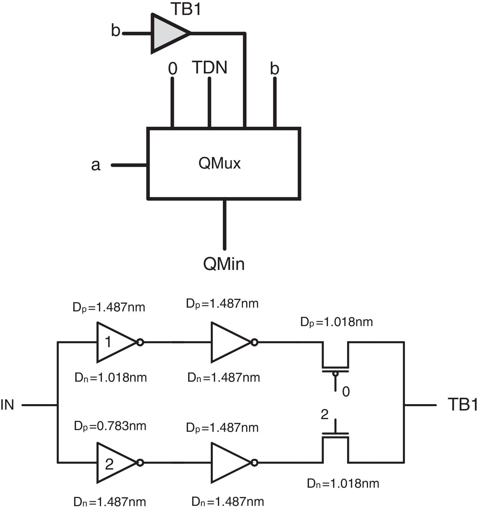
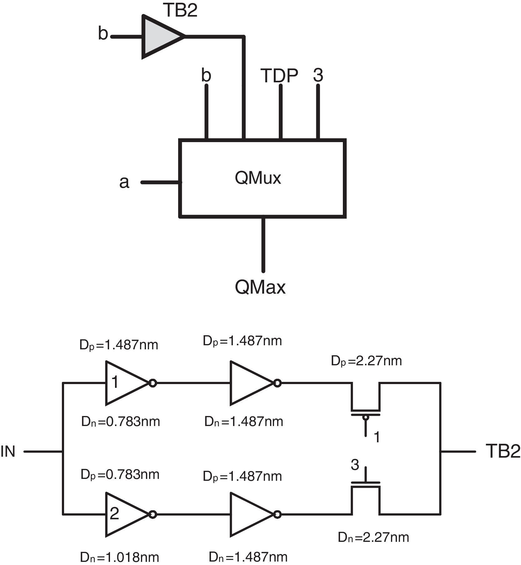
The proposed design can be simplified more by removing the QMux2 module used in the second pin of maximum circuit and the third pin of minimum circuit and replacing each of them by another circuit in order to reach a more hardware-efficient circuit with higher performance. Therefore, two ternary buffer circuits are designed, which can help to achieve the desired outputs with lower number of transistors. As the QMux2 module has been utilized with different inputs in the basic schemas of the proposed minimum and maximum circuits, two different ternary buffers should be used in the second design for minimum and maximum circuits. The main difference between these two buffers is their different required switching thresholds which are obtained by adopting proper diameters in the first level inverters of the buffers.
Figure 6 shows the final proposed minimum circuit and the transistor level schema of its ternary buffer (TB1). This circuit includes specific CMOS-like threshold detector inverters and a voltage division stage according to (Moaiyeri et al., 2011). It is worth pointing out that in the proposed TB1 circuit DN=1.018nm and DP=1.487nm are adopted for the diameters of the n-type and p-type devices in inverter1 and DN=1.487nm and DP=0.783nm are adopted in inverter2. In addition, a 2/3VDD (a 2 logical level) voltage is utilized as the supply in this circuit. Accordingly, the required 0, 1, 2 logics are obtained at the output of TB1 in the proposed minimum circuit.

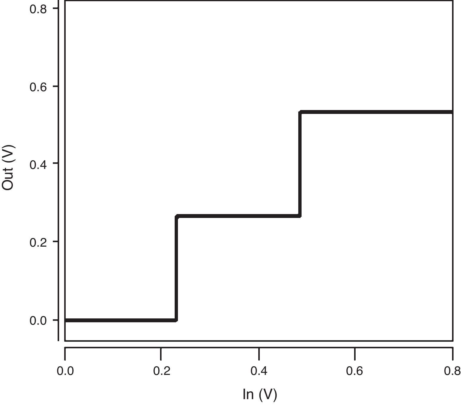
The voltage transfer characteristic (VTC) curve of the ternary buffer used in the proposed QMin circuit is illustrated in Figure 7. As demonstrated in Figure 7, the proposed buffer produces the desired output voltage levels including 0, 1/3VDD and 2/3VDD (VDD=0.8V). In addition, it has a near-ideal VTC with quite steep transition regions which enhance the robustness of the design.
 used in QMin.")
Figure 8 shows the final proposed maximum circuit and the transistor level schema of its ternary buffer (TB2). It is worth pointing out that by selecting DN=1.487nm and DP=0.783nm for the diameters of the n-type and p-type devices in Inverter1 and DN=0.783nm and DP=1.018nm in Inverter2 and using a 1/3VDD supply (a 1 logical value) as the lowest voltage level, the required 1, 2, 3 logics are obtained in TB2 of the maximum circuit.

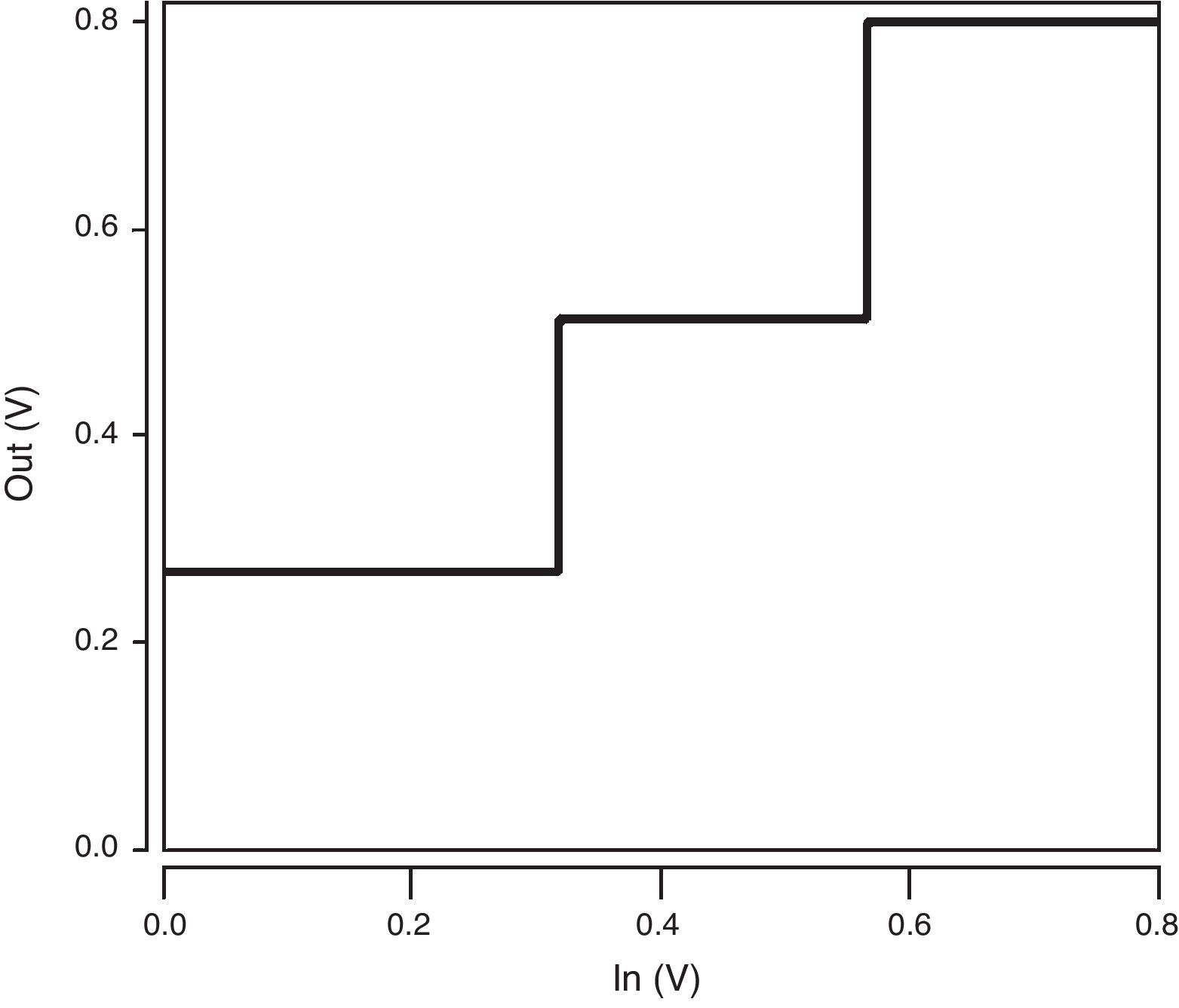
The voltage transfer characteristic curve of the ternary buffer used in the proposed QMax circuit is shown in Figure 9. As illustrated in Figure 9, the proposed buffer produces the desired output voltage levels including 1/3VDD, 2/3VDD and VDD. In addition, it has a near-ideal VTC with quite steep transition regions which enhance the robustness of the design.
4Simulation results and comparison used in QMax.")
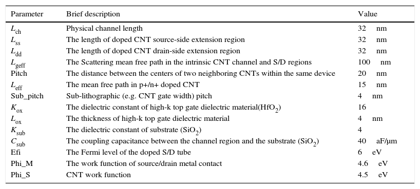
This section discusses the performance of the proposed circuits in different conditions using Synopsys HSPICE with the Stanford compact model CNTFET including all the possible non-idealities at 32nm technology node. This standard model has been developed for unipolar enhancement-mode MOSFET-like-CNTFET, devices in which each transistor may include one or more CNTs as its channel. This model considers the following items idealistically. The Schottky barrier effects at the contacts, inter-CNT charge screening effects, scattering, back-gate effect, gate and source/drain resistances and expansion of doped regions of source/drain (Deng, 2007; Deng & Wong, 2007a, 2007b). Table 2 shows CNTFET model parameters, their values, and a brief explanation.
Some of the important CNTFET model parameters.
| Parameter | Brief description | Value |
|---|---|---|
| Lch | Physical channel length | 32nm |
| Lss | The length of doped CNT source-side extension region | 32nm |
| Ldd | The length of doped CNT drain-side extension region | 32nm |
| Lgeff | The Scattering mean free path in the intrinsic CNT channel and S/D regions | 100nm |
| Pitch | The distance between the centers of two neighboring CNTs within the same device | 20nm |
| Leff | The mean free path in p+/n+ doped CNT | 15nm |
| Sub_pitch | Sub-lithographic (e.g. CNT gate width) pitch | 4nm |
| Kox | The dielectric constant of high-k top gate dielectric material(HfO2) | 16 |
| Lox | The thickness of high-k top gate dielectric material | 4nm |
| Ksub | The dielectric constant of substrate (SiO2) | 4 |
| Csub | The coupling capacitance between the channel region and the substrate (SiO2) | 40aF/μm |
| Efi | The Fermi level of the doped S/D tube | 6eV |
| Phi_M | The work function of source/drain metal contact | 4.6eV |
| Phi_S | CNT work function | 4.5eV |
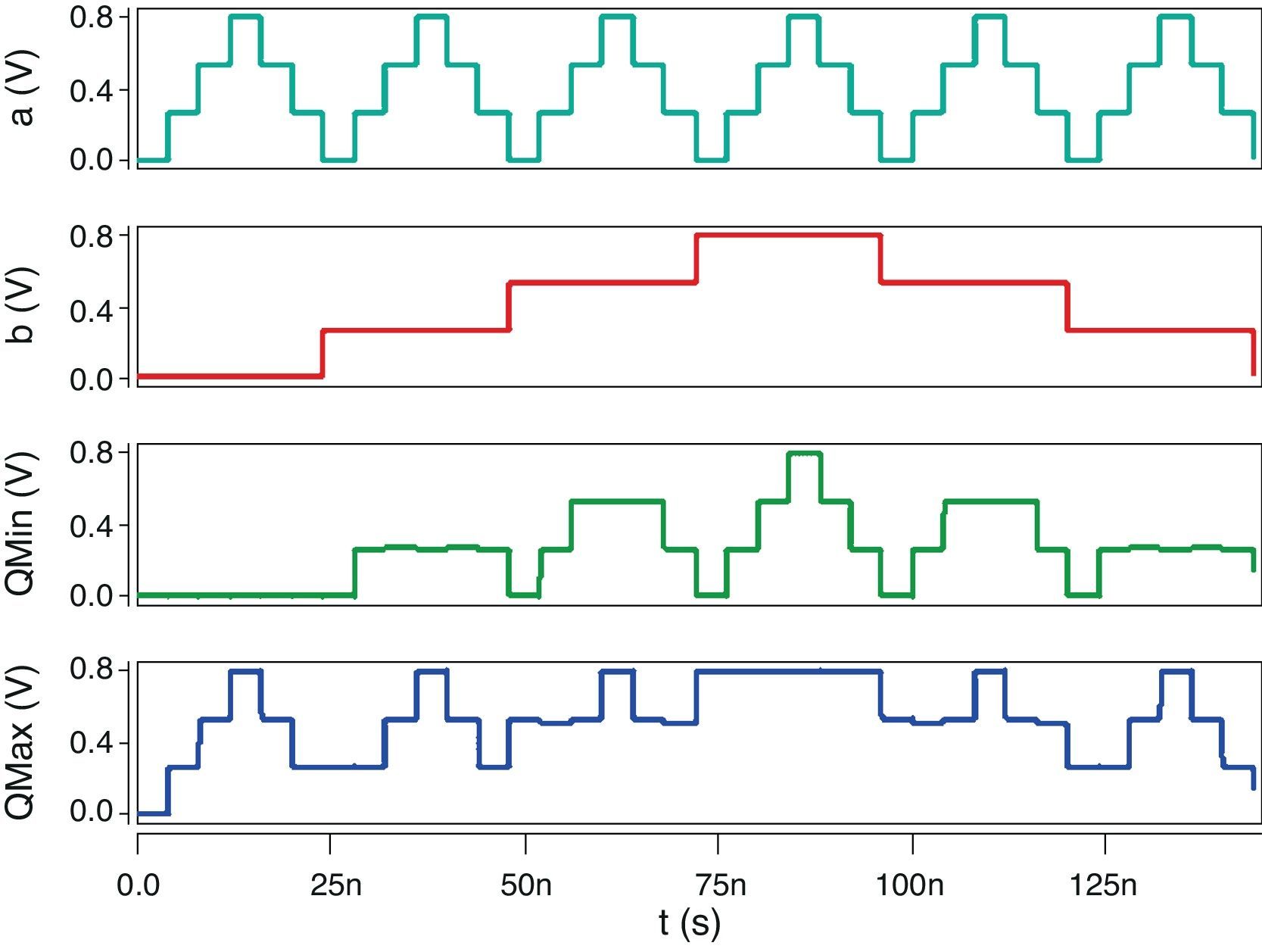
Figure 10 shows the input and output signals of the proposed quaternary logic circuits simulated at 0.8V supply voltage, which authenticates the correct operation of the designs.

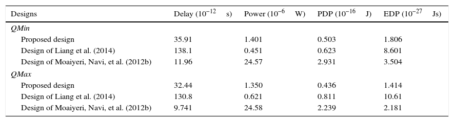
The proposed CNTFET-based quaternary circuits are simulated at 0.8V supply voltage with a 0.5fF load capacitor and the results including propagation delay, power consumption, power-delay product (PDP) and energy-delay product (EDP) are given in Table 3. According to the results, the proposed designs have smaller propagation delays as compared to (Liang et al., 2014), lower power consumption in comparison with (Moaiyeri et al., 2012b) and the lowest PDP and EDP values.
Simulation result of quaternary maximum and minimum circuits.
| Designs | Delay (10−12s) | Power (10−6W) | PDP (10−16J) | EDP (10−27Js) |
|---|---|---|---|---|
| QMin | ||||
| Proposed design | 35.91 | 1.401 | 0.503 | 1.806 |
| Design of Liang et al. (2014) | 138.1 | 0.451 | 0.623 | 8.601 |
| Design of Moaiyeri, Navi, et al. (2012b) | 11.96 | 24.57 | 2.931 | 3.504 |
| QMax | ||||
| Proposed design | 32.44 | 1.350 | 0.436 | 1.414 |
| Design of Liang et al. (2014) | 130.8 | 0.621 | 0.811 | 10.61 |
| Design of Moaiyeri, Navi, et al. (2012b) | 9.741 | 24.58 | 2.239 | 2.181 |
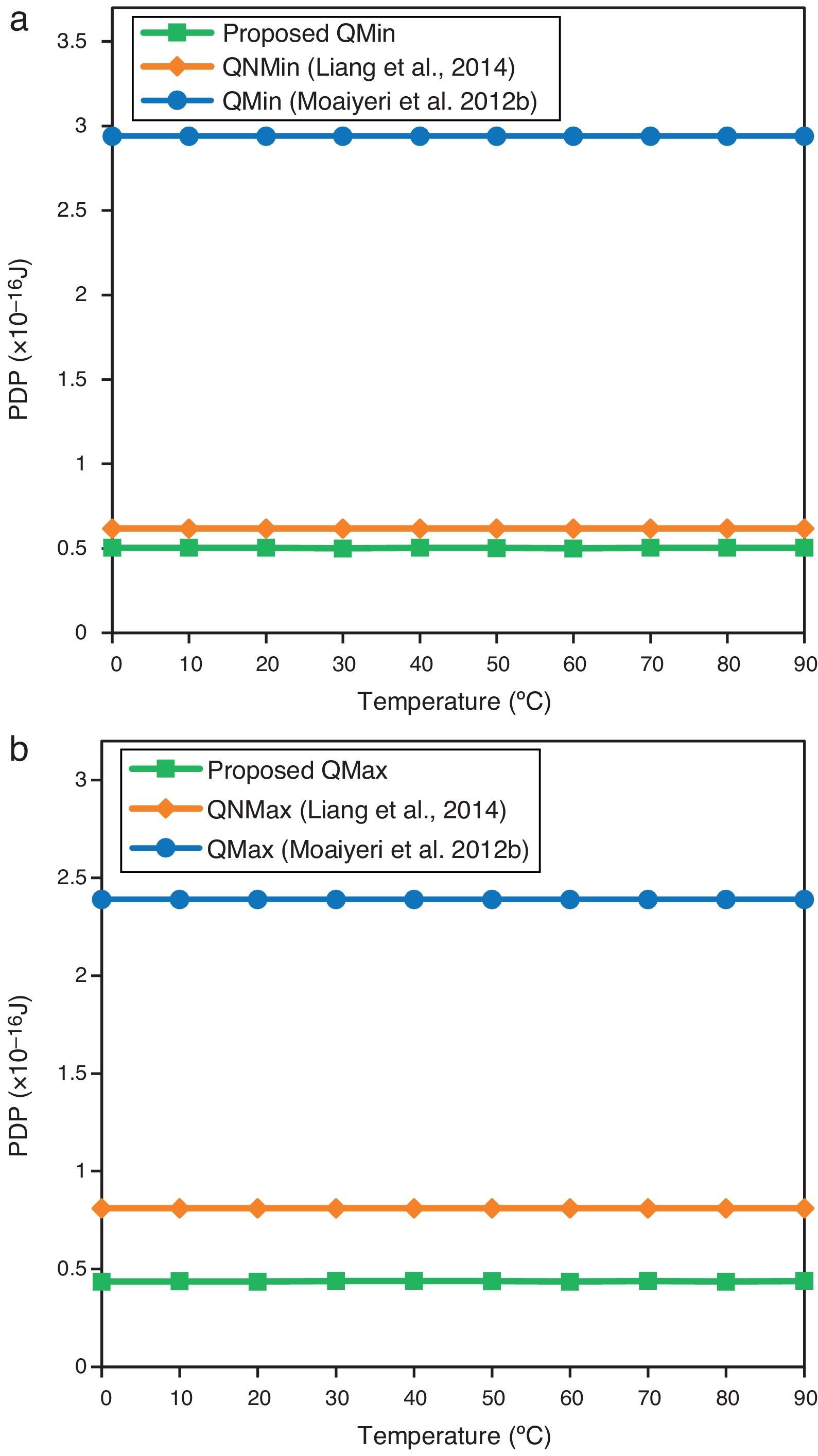
Moreover, the proposed designs are simulated at different ambient temperatures from 0 to 90°C in order to evaluate their operation at different temperatures. The PDP of a CNTFET-based circuit usually does not change significantly by temperature variations because of CNT thermal stability. In addition, as shown in Figure 11, the proposed designs have lower PDP at different temperatures as compared to the other designs.

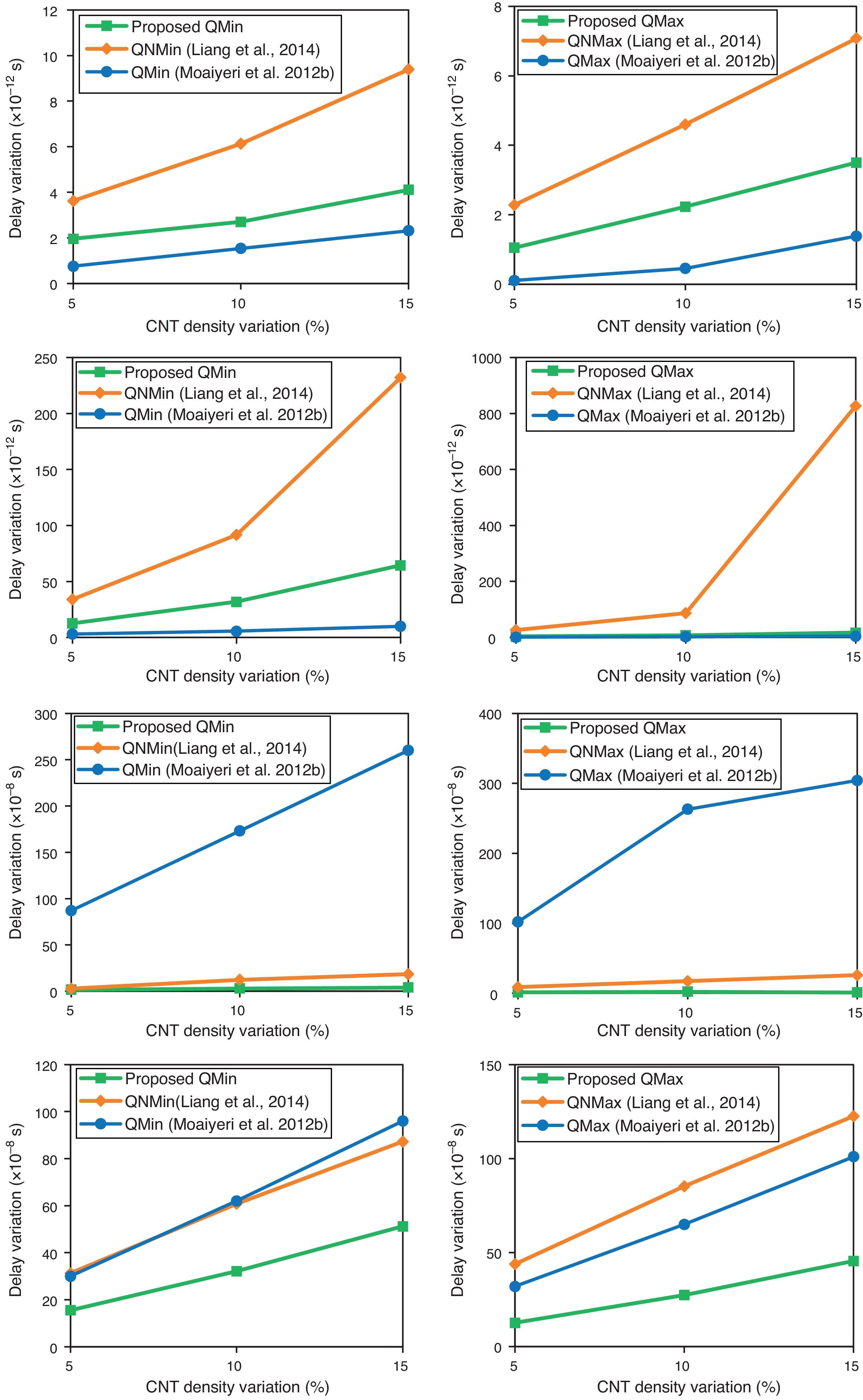
Systematic and random process variations are among the major challenges ahead of nanoscale devices and circuits. As the proposed CNTFET-based quaternary logic circuits are designed based on multiple threshold voltage method, the impact of the process variation that alternates the threshold voltage of the CNTFETs should be definitely studied. As the proposed method is based on multi threshold CNTFETs and the threshold voltage of a CNTFET is dominantly determined by the diameter of its CNTs, the functionality of the proposed quaternary circuit should be evaluated considering CNT diameter variations. In addition, recently, CNT counts variations is proven experimentally to be the most important source of variation in CNTFET circuits (Zhang, Patil, Wong, & Mitra, 2011).
Therefore, the Monte Carlo simulation has been carried out to assess these process variations with ±5% up to ±15% Gaussian distributions and variation at the ±3σ level. Figure 12 shows the results of this simulation. According to the results, the proposed CNTFET-based logic circuits are very low sensitive to process variations, especially in terms of power variations.
5Conclusions
As the nanotechnology-based multiple-valued logic design is concerned, energy-efficient min–max circuits have been proposed based on CNTFETs with multi threshold voltages based on the CNTFET's unique properties. The simulation results certify authenticity of the proposed method as a superior proposed quaternary minimum and maximum circuit, especially in terms of PDP and EDP, as compared with other circuits under different simulation conditions and in the presence of process and temperature variations. The proposed designs leads to 51% and 63% lower PDP and 64% and 61% lower EDP, respectively as compared to the state-of-the-art CNTFET-based quaternary circuits presented in the literature. In future work we expect to develop the proposed method for implementing complex arithmetic operations and designing an efficient quaternary ALU. Also, we expect that the proposed method can be generalized effectively for radices higher than four.
Conflict of interestThe authors have no conflicts of interest to declare.
Peer Review under the responsibility of Universidad Nacional Autónoma de México.