


Pure and niobium doped bismuth titanate ceramics Bi4Ti3−xNbxO12(Nb−BiT) with x ranging from 0% to 2% are prepared by sol–gel method. Pellets are sintered by pressureless sintering (PLS) and spark plasma sintering (SPS). Raman spectroscopy indicates distortion in the structure due to the substitution of titanium by niobium. X-ray photoelectron spectroscopy (XPS) displays the Nb integration to the bismuth titanate ceramic structure. X-ray diffraction shows no secondary phases and offers clues about crystallographic texturing due to the SPS technique. The shape and size of the grains are strongly influenced by the niobium added to the system as reported by scanning electron microscopy. Ferroelectric hysteresis loops exhibit the effect of the niobium and the texturing on the ferroelectric behavior. Higher values of remanent polarization are reported for PLS samples. In comparison with PLS, higher values of the relative permittivity are reported for SPS samples due to the non-homogeneous incorporation of Nb.
El titanato de bismuto puro y dopado con niobio Bi4Ti3−xNbxO12(Nb−BiT), en un rango de x entre 0 a 2%, es obtenido por el método sol-gel. La densificación de las muestras cerámicas se desarrolla por medio de sinterizado tradicional y asistido por arcos eléctricos. La espectroscopia Raman reporta evidencia de la distorsión en la estructura debido a la sustitución de titanio por niobio. La espectroscopia de fotoelectrones emitidos por rayos X muestra la integración del niobio en la estructura cerámica de titanato de bismuto. La difracción de rayos X no muestra fases secundarias y ofrece pistas sobre la textura cristalográfica debido a la técnica de sinterizado asistido por arcos eléctricos. La forma y el tamaño de los granos están fuertemente influidos por el niobio agregado al sistema, según lo reportado por la microscopia electrónica de barrido. Los lazos de histéresis ferroeléctrica exhiben el efecto del niobio y la textura sobre el comportamiento ferroeléctrico. Se reportan valores más altos de polarización remanente para muestras obtenidas por sinterizado tradicional. En comparación con el sinterizado tradicional, las muestras obtenidas por sinterizado asistido por arcos eléctricos muestran los valores más altos de la permitividad relativa debido a la distribución no homogénea de la incorporación del niobio.
Bismuth layer-structured ferroelectrics (BLSFs) are good candidates for developing lead-free piezoelectric materials [1–6]. In the BLSFs family, bismuth titanate (BiT) is well known due to its high dielectric constant, Curie temperature (675°C) (Tc), anisotropy, and other properties. Therefore, BiT is considered attractive for high temperature piezoelectric devices, memory storage and optical displays [2,7,8].
The sol–gel method offers considerable advantages compared to other synthesis techniques, such as: excellent chemical stoichiometry and a lower crystallization temperature due to chemical efficiency at the molecular level. Then, a better solid solution is to be expected in comparison with solid state reactions [3,9]. Doping BiT to obtain improved properties is still an issue [10,11]. When doping with sol–gel, better dissolution between BiT and dopant has been reported [12,13]. To improve the ferroelectric properties of BiT, ion substitutions with other cations like niobium and lanthanum have been investigated [14–17]. It has been shown that doping with donor cations like Nb in the Ti position (NbTi .) decreases electrical conductivity and improves ferroelectric and piezoelectric properties of BiT ceramics [2,18]. Dopped BiT has also reached other field like luminescence when doping with ytterbium and holmium [19].
The application of sintering techniques plays an important role in the improvement of BiT ceramic properties [6]. Spark plasma sintering (SPS) has been proven to be an efficient technique to control ceramic structures [20–24]. Bi2/3Cu3Ti4O12 has been successfully sintered by electric field-assisted flash sintering [22]. An effective characterization method is also important to study dopped BiT ceramics. In the literature, the most used techniques capable of providing information about doping are Raman spectroscopy and X-ray photoelectron spectroscopy (XPS). These techniques have provided useful information to characterize Bi4Ti3O12-based ferroelectric polycrystalline ceramics [23] and lanthanum-doped strontium bismuth titanate [24]. A compendium for Raman phonon modes frequencies for bismuth titanate is reported by Mukhortov et al. [25].
In the present work, niobium doped bismuth titanate ceramic is investigated Bi4Ti3−xNbxO12(Nb−BiT) with x ranging from 0% to 2%. The experimental procedure is devoted to describing the sol–gel process, sintering, and characterization. The discussion of results is divided into three subsections. Nb incorporation to the ceramic structure is carefully revised trying to find new insights to better understand the role of Nb at the atomic level. Grain morphology and evidence of crystallographic texture are analyzed. Special attention is focused on SPS samples of Nb-doped BiT. Finally, the ferroelectric hysteresis loop and the dielectric permittivity are also investigated.
Experimental procedureNitrate penta-hydrated bismuth BiNO33⋅5H2O, Alfa Aesar, 98% purity are mixed with acetic acid (CH3COOH, JT Baker, 99% purity) with a molar ratio equal to 1:3. During magnetic stirring, deionized water (H2O, 99% purity) is added with a molar ratio of Bi:H2O=1:6. Separately, titanium isopropoxide (TiO4C12H28, Alfa Aesar, 97% purity) is poured on 2-methoxyethanol (C3H8O2, Alfa Aesar, 99% purity) with a molar ratio of 1:30 [26].
Next, the solutions are mixed in one beaker and magnetic stirrer for 30min at 40°C. Following this, acetylacetone (C5H8O2, Sigma Aldrich, 99% purity) is added and stirred magnetically for 30min. The solution is then allowed to rest for 18h at room temperature (RT) without magnetic stirring, followed by a further 40h of magnetic stirring; gelation takes place, and the gel is aged for 48h. Finally, the gel is dried at 150°C for 24h to obtain a powder, which is subjected to grinding in a traditional mortar and pestle, before being calcined at 750°C for 4h to obtain bismuth titanate crystal phase. For the case of niobium doped system, niobium chloride (NbCl5, Alfa Aesar, 99.95% purity) is poured into the glass with 2-methoxyethanol (C3H8O2) on the magnetic stirrer for 7min before pouring titanium isopropoxide (TiO4C12H28). The molar ratio of the dopant with respect to titanium contributor is defined by the formula Bi4Ti3−xNbxO12, wherein the criterion for doping system is 0.5%, 1%, 1.5% and 2mol% of niobium [27].
The powder compact pellets are sintered by pressureless sintering (PLS) and spark plasma sintering (SPS). The green pellets made to be sintered by PLS are pressed at 35MPa. They are sintered at 1000°C for 8h. The SPS samples are carried out using 1.4g of powder, applying 500A, pulse switch on/off 12/2, and 5kN load. The crystal structure and morphology of the powders and pellets are analyzed by X-ray diffraction (XRD) in a PANalytical X’Pert PRO. Raman spectroscopy is performed by WITec Focus Innovation. The morphology and the size of particles and grains are analyzed by scanning electron microscopy (SEM) in a JEOL JSM 7000F (JEOL Tokyo, Japan). Additionally, particle and grain size are statistically measured with freely available software ImageJ by taking a micrograph obtained with 2000× magnification, which allowed for the counting of around 100 particles or grains. To analyze morphology, higher magnifications of 20,000 micrographs are taken. XPS analysis is carried out using an ESCALAB 250Xi Thermo Scientific spectrometer with a monochromatic Al Kα anode (1486.7eV) with a resolution of 0.45eV. Crystallite size is estimated with Scherrer's formula, relative density is obtained with Archimedes method, ferroelectric hysteresis loops are analyzed using 25kV/cm over pellets with precision ferroelectric tester system by Radiant Technologies Inc.
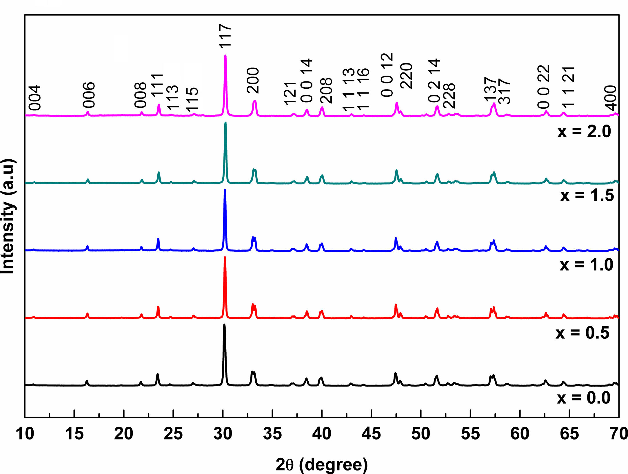
Results and discussionPowder characterizationNiobium doped bismuth titanate Bi4Ti3−xNbxO12(Nb−BiT) is obtained with Nb added quantities in the range of x from 0% to 2%. The obtained powders are free of secondary phases as observed in the XRD patterns (reference pattern: pdf 01-073-2181), see Fig. 1. This is an expected result because Ambriz-Vargas et al. [27] report that BiT can be dopped with Niobium up to x=2%. The compounds have an orthorhombic crystal system [12,26] with space group Fmmm and the lattice parameters are a=5.4100 Å, b=5.4480 Å and c=32.8400 Å. The XRD patterns are congruent with the existence of perovskite structure in agreement with other investigations [14,15].

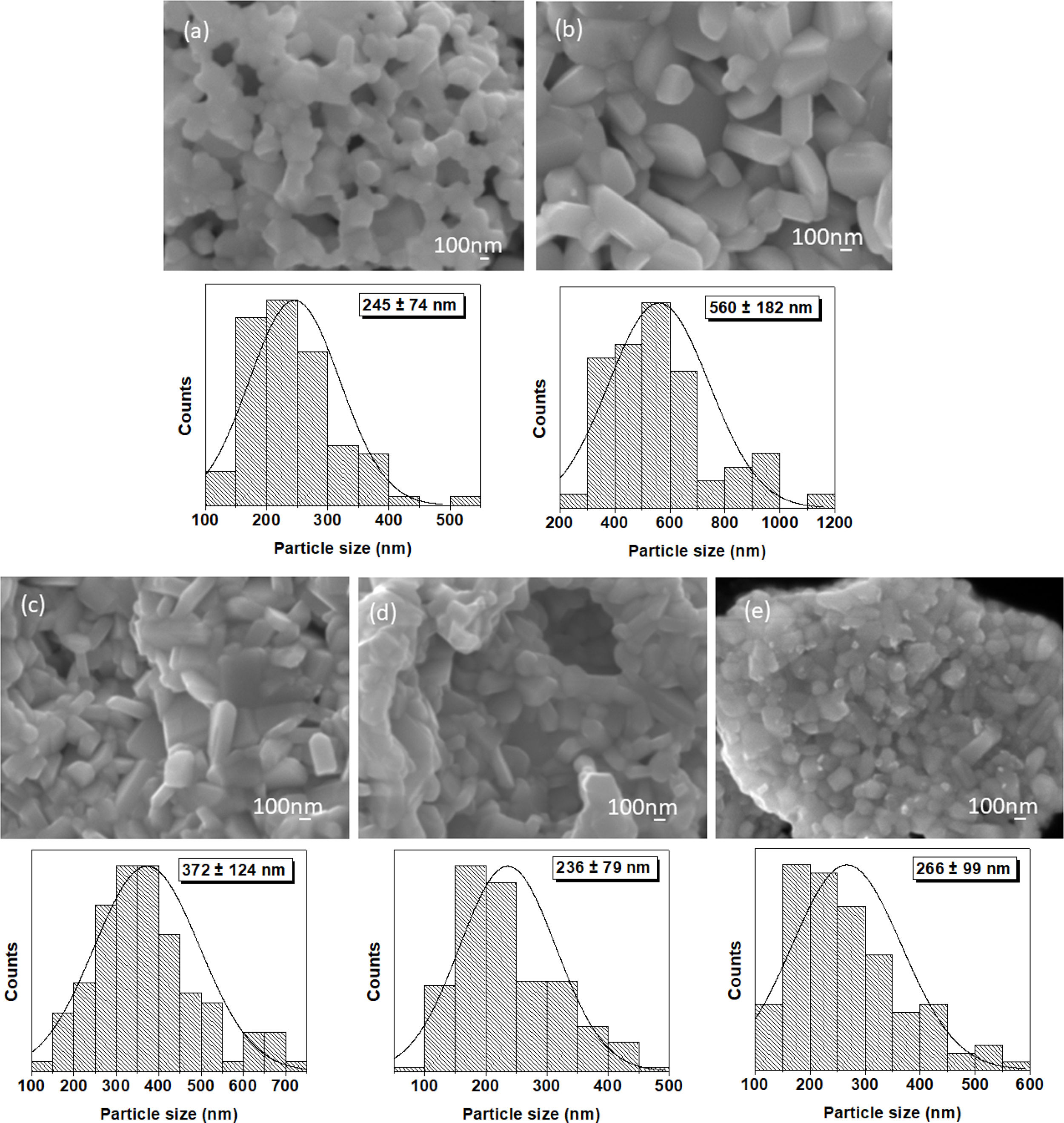
It is found that the crystallite size is influenced by the Nb dopant concentration, i.e., for x equals to 0.0, 0.5, 1.0, 1.5 and 2.0, the corresponding crystallite size is 101.82, 181.57, 140.60, 99.19, and 88.15nm, respectively. The crystallite size increases from x=0.0 to x=0.5. Thus, as the Nb dopant further increases, the crystallite size decreases. The set of micrographs with their corresponding histograms for particle size (see, Fig. 2) shows the powder morphology and particle size. As usual in sol–gel, nanoparticles agglomerates are obtained. For x=0, nearly spherical particles can be observed with grain size equal to 245±74nm (see Fig. 2a). Then, for x=0.5, plate-like morphology is perceived with the larger dimension equal to 560±182nm (see Fig. 2b). In the cases of x equal to 1.0, 1.5, 2.0 (see Fig. 2c–e), the grain size shows a tendency to decrease [28–30] as can be seen for the grain sizes values 372±124, 236±179, and 266±99nm, respectively. It is probable that a fraction of the Nb atoms is located at the grain boundaries of the particle agglomerates, pinning them and avoiding boundaries displacement and grain growth [31,32].
 x=0.0, (b) x=0.5, (c) x=1.0, (d) x=1.5, and (e) x=2.0.")
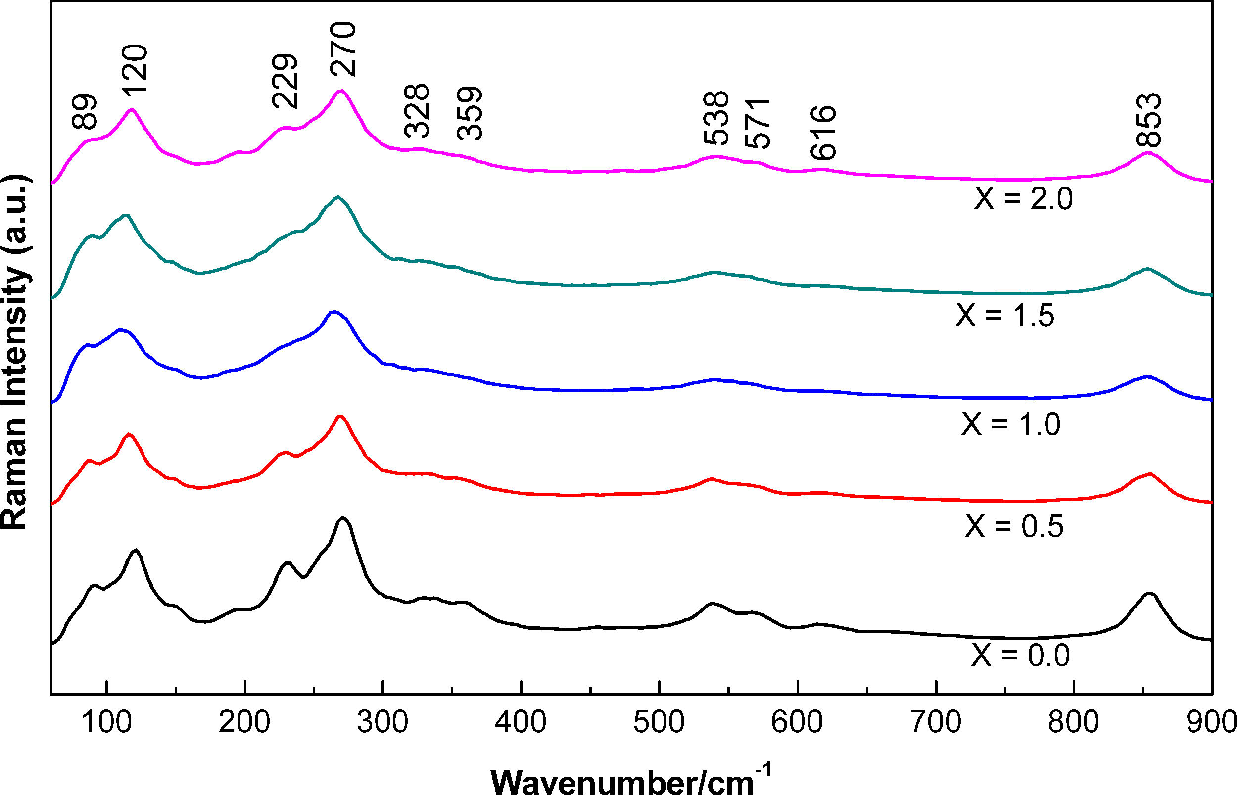
Fig. 3 shows the Raman spectra of bismuth titanate powders with different Nb dopant concentrations. According to previous investigations [12,29,30], significant changes mainly in modes 328, 359, and 571cm−1 can be attributed to distortions in the structure due to the substitution of titanium by niobium in the TiO6 octahedral complexes [14,18,27,31,33]. In addition, the 89 and 120cm−1 modes are changing with Nb concentration due to the undergoing modifications in the octahedron and the influence on the bismuth–oxygen links. The 229cm−1 mode is related to the vibration of OTiO, and the 270cm−1 mode describes the torsional vibration of TiO within the octahedron TiO6[34]. The modes 538, 616 and 853cm−1 are connected to the high energy that exists in the bending vibrations within the octahedron TiO6[34], the 571 and 853cm−1 modes match the stretching vibrational modes OTiO [30,32], and the 270, 538 and 853cm−1 modes indicate the presence of a perovskite structure [35–37]. The 229cm−1 mode exhibits a widening with the increase of Nb concentration due to titanium substitution [14,18,27]. Finally, for the modes 89 and 120cm−1, the peaks become wider as the concentration of Nb increases, this is due to the influence of the distorted octahedron and the bismuth–oxygen links [18].

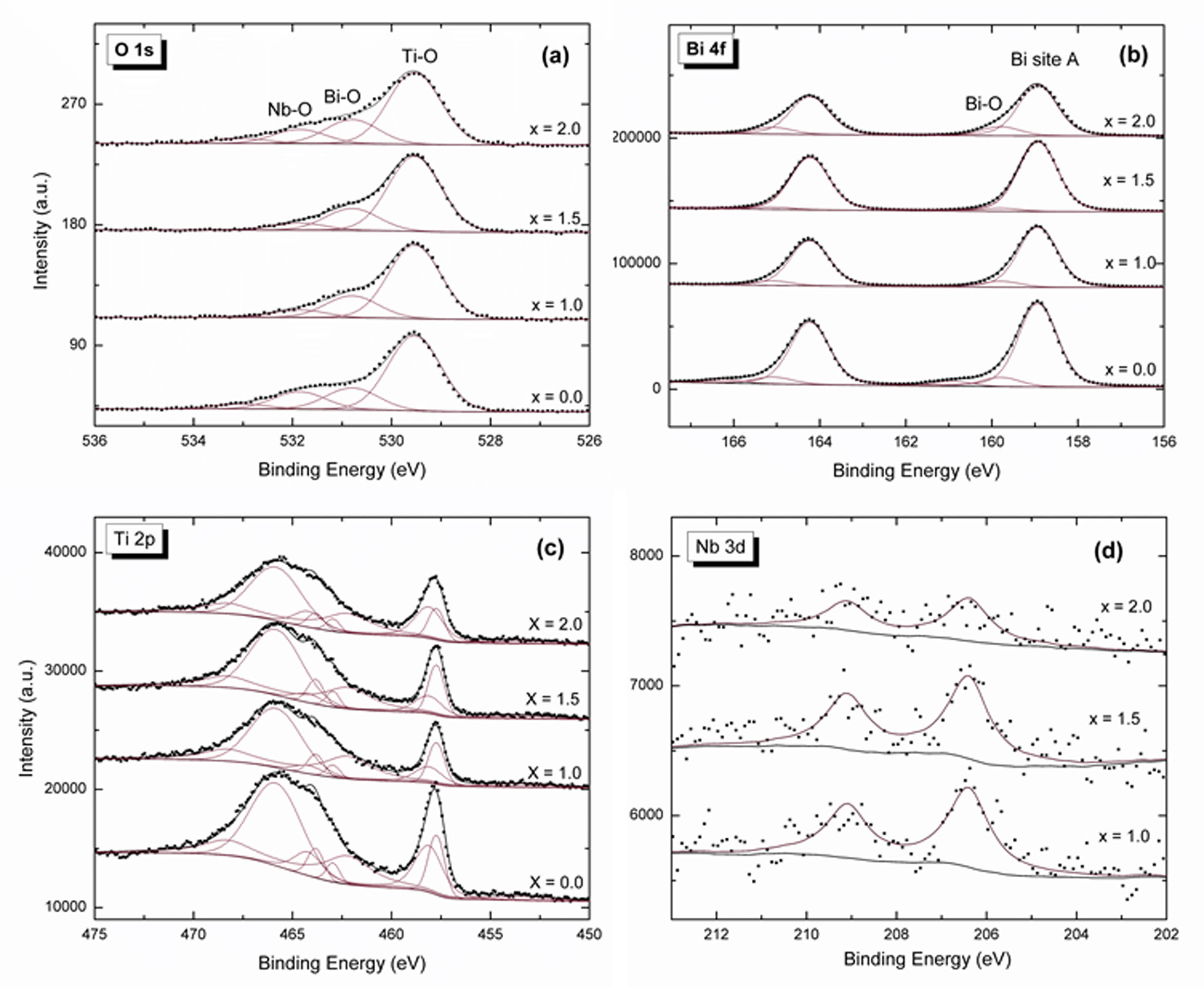
Fig. 4 shows XPS measurements. Nb 3d, O 1s, Ti 2p, and Bi 4f core levels are obtained for x equal to 1.0, 1.5 and 2.0 powders. O 1s is used for aligning all spectra. The signal in Fig. 4a is attributed to four peaks associated with TiO at 529.5eV, BiO at 530.8eV, NbO at 531.8eV (Nb was bonded as Ti substitution due to orthorhombic structure) [38,39], and CO or oxygen that is absorbed by the surface at 533eV. The Bi 4f (Fig. 4b) presents two signals. The first signal at 158.9eV is related to bismuth at the perovskite orthorhombic structure, and the second one at 159.8eV is connected to bismuth oxide due to bismuth layered structure. In Fig. 4c, Ti 2p has four signals (453.6, 457.7, 458 and 462.2eV) associated to titanium signal as Ti1+, Ti2+, Ti3+ and Ti4+, respectively, and two more related to Bi 4d3/2 (462.9, 465.8eV). These last two can be correlated to bismuth oxide in the bismuth layered structure. The Ti4+ signal decreases due to substitution by Nb3+ at the titanium atoms position. The two Bi 4d signals are associated to the bismuth of the titanate structure and bismuth oxide which are also presented in Bi 4f core level. The Nb 3d signal (Fig. 4d) tends to increase with the Nb doping until x=1.5, whereas for x=2.0 the peak intensity decreases.
, Bi 4f (b), Ti 2p (c), and Nb 3d (d) region for Nb-doped bismuth titanate ceramics powder with 0.0≤x≤2.0.")
Raman spectroscopy and XPS measurements can be employed for analyzing the Nb incorporation to the bismuth titanate crystal lattice. A relation is observed for the Ti4+, Nb 3d signals, and the Raman 229cm−1 mode. For these three cases, it is not straightforward to attribute a defined tendency for the peak behavior [12]. For x from 0 to 1.5, the Ti4+, Nb 3d signals increase and the 229cm−1 mode intensity decreases. Further, for x from 1.5 to 2.0, the opposite behavior can be observed, i.e., the Ti4+, Nb 3d signals decrease and the 229cm−1 mode intensity increases. This behavior can be attributed to a Nb solid solubility limit in the Bismuth Titanate (BiT) lattice or a change in the thermodynamic equilibrium for x=1.5.
Additionally, for x from 0 to 1.5, a major part of the added niobium tends to incorporate into the BiT solid network. As x increases from 1.5 to 2.0, the fall in the Ti4+, Nb 3d signals allows the authors to conclude that Nb atoms cannot dissolve in the BiT network with the increase of x values. In fact, for x equal to 1.0, 1.5 and 2.0, Nb contents are detected as 1.97%, 1.83%, and 1% respectively. Nb atoms are also expected to be incorporated to the grain boundaries. As x increases from 0.5 to 2.0, the grain size decreases because of the Nb pinning effect mentioned above.
In summary, the authors determine that there is a thermodynamic competition between Nb solubility in the BiT network and the Nb incorporation to grain boundaries. The solubility is favored for x<1.5, whereas the grain boundary incorporation is favored for x>1.5.
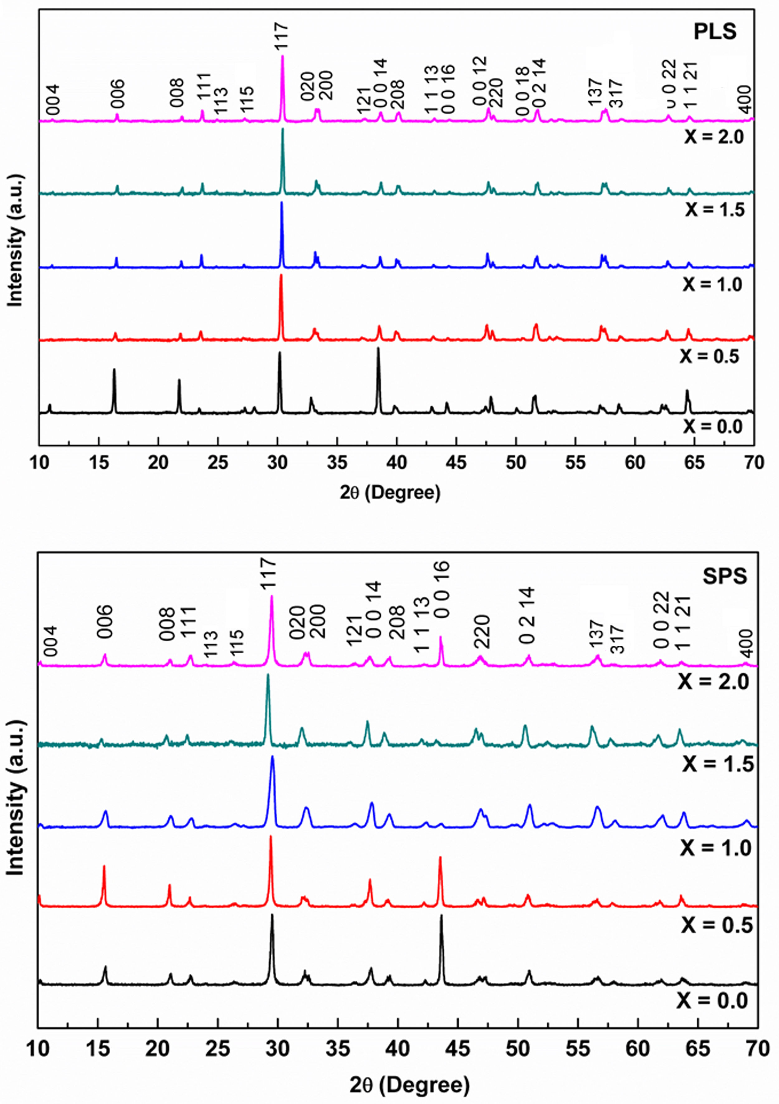
Sintering characterizationFig. 5 shows the set of XRD patterns for PLS and SPS sintered pellets. For PLS, a change in the peak intensity is observed which can be attributed to a change in the crystallographic texture [14] as the Niobium concentrations change. This phenomenon is a result of particle accommodation which takes place during uniaxial pressing of the green body, and the plate-like morphology that develops during sintering. The PLS sample x=0.0 shows strong diffraction peaks from [001] planes in the peaks: (006), (008), (0014), (220), and (1 1 21); while the patterns for PLS with x equal to 0.5, 1, 1.5, and 2.0 of Nb concentration show a weak [001] peaks. Similar results have been previously reported in Ref. [40]. The crystallite size is influenced by the dopant level, i.e., for x equal to 0.0, 0.5, 1.0, 1.5, and 2.0, the corresponding crystallite size is 126.26, 105.52, 135.53, 205.36, and 90.12nm, respectively. Therefore, the crystalline structure of the PLS samples is affected by the Nb doping.
 and SPS (down) in the range of x equal to 0.0, 0.5, 1.0, 1.5, and 2.0.")
XRD patterns for SPS pellets show crystallographic texture for almost all samples. This effect can be clearly seen for x between 0.0 and 1.0. The patterns show strong diffraction peaks from [001] planes as follows: for x=0.0, preferred peaks orientation can be seen for (006) and (0 0 16); for x=0.5, the preferred oriented peaks are (006), (008), (0 0 14), and (0 0 16); for x=1.0, we see peaks (006), (0 0 14) and (220) preferred oriented. In addition, in a lesser measure, preferred oriented peaks can also be observed for x=1.5 (0 0 14) and for x=2.0 (0 0 16).
On the other hand, it is observed that the crystallite sizes in the SPS pellets are 90, 105.50, 90, 70, and 65.5nm for x equal to 0.0, 0.5, 1.0, 1.5, and 2.0, respectively. The pattern for the PLS reveal a strong texture in planes [001] when x=0.0, whereas the patterns for the PLS for x equal to 0.5, 1.0, 1.5, and 2.0 shows less orientation in [001] planes. The SPS for x equal to 1.0, 1.5, and 2.0 shows less orientation in [001] planes than the SPS for x=0.0 and x=0.5. The XRD patterns of PLS and SPS when x=0.0, and the pattern of SPS when x=0.5 exhibit strongly enhanced [001] peaks which indicate the c-axis is perpendicular to perovskite-like layers in the BiT [40].
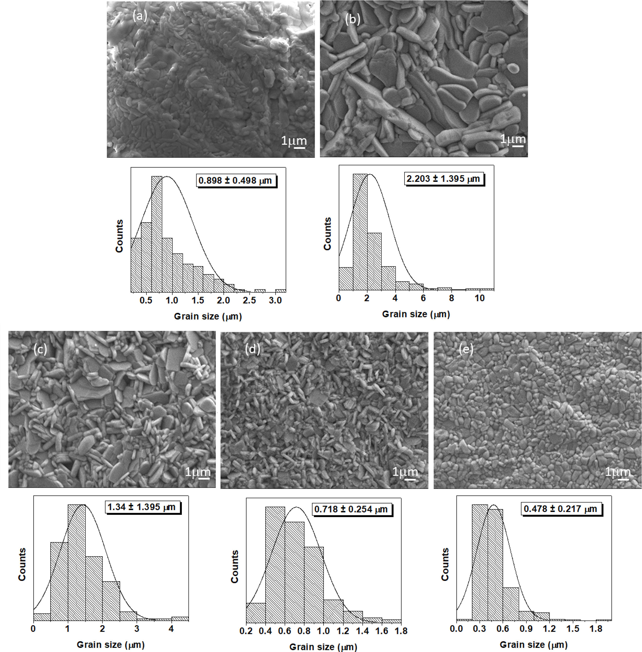
Figs. 6 and 7 illustrate representative SEM micrographs with the related grain size histogram for PLS and SPS sintered ceramics, respectively. For both cases, x runs from 0.0% to 2.0%. Table 1 reports the mean grain size and the standard deviation for the above-mentioned samples. It can be observed the difference in the grain sizes between the PLS and SPS specimens. As a tendency, PLS particle sizes are larger than SPS ones. This result can be attributed to the fact that, for PLS, the larger firing time and higher temperature promotes grain growth, whereas, for SPS specimens, temperature rise has a slight effect on the microstructure due to the high heating rate and short dwelling time of the process [41,42]. As can be observed in Table 1, grain size decreases as the Niobium dopant concentration increases for PLS. On the other side, for SPS, mean grain size increases from x=0.0 to x=0.1, and as x further increases, mean grain size decreases.
 and grain size histograms (bellow) for Nb-doped bismuth titanate specimens sintered by PLS (a) x=0.0, (b) x=0.5, (c) x=1.0, (d) x=1.5, and (e) x=2.0.")
 and grain size histograms (bellow) for Nb-doped bismuth titanate specimens sintered by SPS (a) x=0.0, (b) x=0.5, (c) x=1.0, (d) x=1.5, and (e) x=2.0.")
Mean grain size and standard deviation for sintered samples obtained by PLS and SPS as a function of the dopant concentration x.
| Sample | PLS (μm) | SPS (μm) | ||
|---|---|---|---|---|
| Mean | SD | Mean | SD | |
| x=0.0 | 5.079 | 2.072 | 0.898 | 0.498 |
| x=0.5 | 4.525 | 2.224 | 2.203 | 1.395 |
| x=1.0 | 2.218 | 0.800 | 1.434 | 0.656 |
| x=1.5 | 1.760 | 0.761 | 0.718 | 0.254 |
| x=2.0 | 0.857 | 0.348 | 0.478 | 0.217 |
The grain morphology is strongly influenced by the Nb dopant concentration. Plate-like morphology is obtained for most of the PLS (Fig. 6a–d) and SPS (Fig. 7a–d) samples and it can be connected to preferential direction during grain growth because of the bismuth titanate crystal structure. The plate-like morphology is usual for the Aurivillius phase structure [43,44].
Herein, for x=2.0, it can be observed that grain morphology has almost achieved a round-like shape for both PLS and SPS techniques. This result seems to be not very common in what have been reported up today. Most of Aurivillius phases keep its plate-like morphology even with dopants [10,11,43,45]. Therefore, grain growth inhibition during sintering of Nb-BiT influences the grain morphology. As previously mentioned, the pinning effect of Nb at the grain boundary is supposed to inhibit grain growth.
In Fig. 7, the SPS micrographs show the grain morphology behavior with Nb doping is quite similar to the one obtained for sol-gel synthesized particles (Fig. 2). This is an expected result considering that SPS is a fast technique where the limited time frame nearly keeps the morphology of the starting powders. Besides, it can be observed that the formation of particle neck and the low porosity. In fact, the relative density of almost 100% is reached. The relative densities of the SPS pellets are 100% for x=0.0 (Fig. 7a), x=0.5 (Fig. 7b), x=1.0 (Fig. 7c), and x=1.5 (Fig. 7d), and it is 98.66% for x=2.0 (Fig. 7e). Hence, we can conclude that the Nb dopant effect is dominant for both sintering techniques. In addition, for PLS, lower density values are reached. For PLS pellets, the relative density values 90.93%, 91.59%, 94.84%, 92.79%, and 90.68% were achieved for x equal to 0.0, 0.5, 1.0, 1.5, and 2.0, respectively.
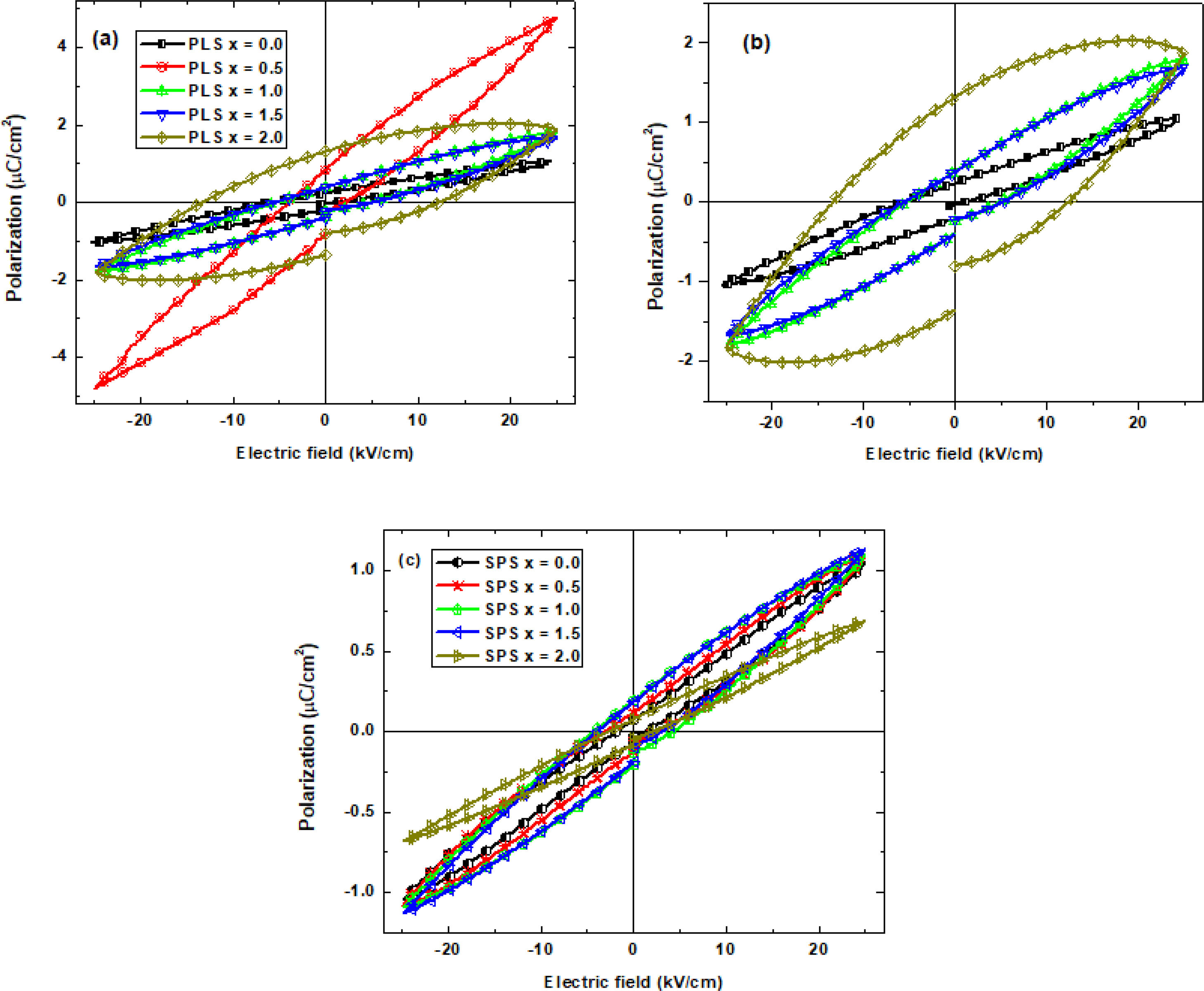
Ferroelectric and dielectric propertiesThe set of PLS hysteresis loops (P–E loops) in the Fig. 8a displays a higher ferroelectric response than the SPS (Fig. 8b). This can be possible because the crystallographic texture [46] of the SPS samples favors the (001) directions (c-axis) [47] (see, Fig. 5). The polarization in BiT develops along the crystallographic directions (100) and (010) (a–b axes) as reported in Ref. [47]. Therefore, crystallographic texture with preferred distribution along the axial direction is not expected to favor polarization [34,37]. Hysteresis loops are measured along the axial direction. On the other side, PLS samples show a more random crystallographic texture (Fig. 5) giving more chances to have crystal directions (100) and (010) to be oriented along the sample axial direction.
 and (b) PLS specimens and (c) of SPS specimens. For PLS techniques, the samples x=0.0, 1.0, 1.5. and 2.0 are shown separately again due to the scale difference with x=0.5.")
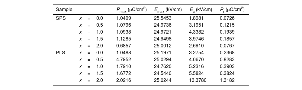
As can be seen in Fig. 8, the loops of all PLS (except for x=2.0) and SPS samples show sloped and elliptic behavior characteristic of polycrystalline soft ferroelectric materials with small coercivity and higher contribution of the dipolar polarization (linear contribution) with respect to those contribution of the orientation polarization (no linear) due to spontaneous polarization. Moreover, these samples do not show loss by dielectric or conductivity phenomena (see below). Table 2 shows the maximum values for polarization (Pmax) at maximum applied electric field (Emax) for PLS and SPS samples. In addition, the values of the coercive electric field (Ec) and remanent polarization (Pr) are reported. From Table 2, it can be observed that the values for coercive field experiences wider changes for PLS than for SPS samples. As has been already mentioned, PLS process takes longer time than SPS, then, the effect of the dopant concentration has a larger time frame to induce a more pronounced difference in the microstructure for PLS samples (Fig. 6) than those of the SPS samples (Fig. 7). A similar picture can be noticed for Pmax, and Pr. It is worthy to mention that this tendency is especially pronounced for the remanent polarization since that Pr values exhibit a higher sensitivity to the Nb doping level. In addition, it can be noted, that there are no significant changes in the Pmax, and Pr values with Nb doping for SPS samples with respect to undoped SPS sample. Whereas an increase of Pmax with the increase of the Nb concentration is observed for the PLS samples and the noticeable increase for x=0.5 is ascribed to its higher grain size discussed above. Moreover, the P-E loop of the PLS sample for x=2.0 exhibits significantly higher coercivity and remanent polarization. However, the loop shows a small decrease of the maximum polarization at the higher values of the applied electric field (>20kV/cm) which can be due both by dielectric loss and/or conductivity along the grain boundaries.
Values of the maximum polarization (Pmax), coercive field (Ec), and remanent polarization (Pr) obtained from the P–E loops for all PLS and SPS specimens.
| Sample | Pmax (μC/cm2) | Emax (kV/cm) | Ec (kV/cm) | Pr (μC/cm2) | |
|---|---|---|---|---|---|
| SPS | x=0.0 | 1.0409 | 25.5453 | 1.8981 | 0.0726 |
| x=0.5 | 1.0796 | 24.9736 | 3.1951 | 0.1215 | |
| x=1.0 | 1.0938 | 24.9721 | 4.3382 | 0.1939 | |
| x=1.5 | 1.1285 | 24.9498 | 3.9746 | 0.1857 | |
| x=2.0 | 0.6857 | 25.0012 | 2.6910 | 0.0767 | |
| PLS | x=0.0 | 1.0488 | 25.1971 | 3.2754 | 0.2368 |
| x=0.5 | 4.7952 | 25.0294 | 4.0670 | 0.8283 | |
| x=1.0 | 1.7910 | 24.7620 | 5.2316 | 0.3903 | |
| x=1.5 | 1.6772 | 24.5440 | 5.5824 | 0.3824 | |
| x=2.0 | 2.0216 | 25.0244 | 13.3780 | 1.3182 | |
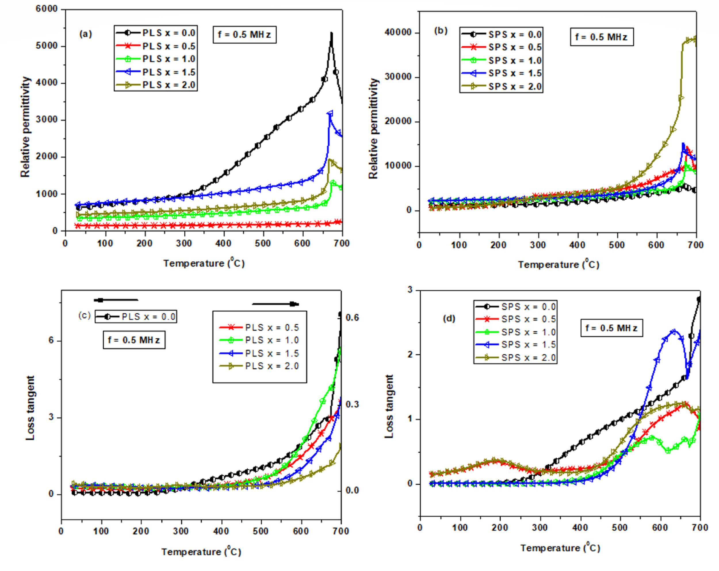
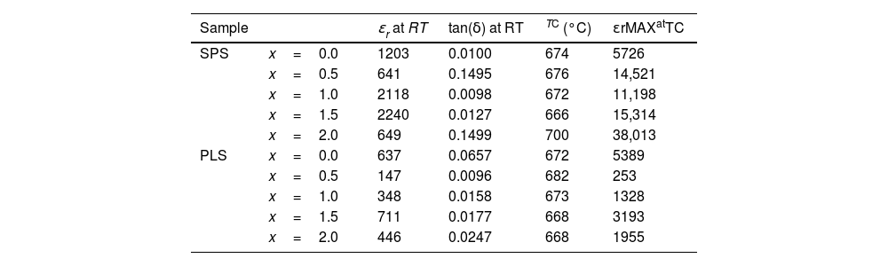
Finally, Fig. 9 shows the relative permittivity (εr) and the loss tangent (tan(δ)) behaviors obtained at 0.5MHz as function of temperature for PLS (Fig. 9a and c) and SPS (Fig. 9b and d) samples, respectively. Table 3 reports the room temperature (RT) relative permittivity and Curie temperature (TC) values. It can be noted that the ferroelectric-paraelectric phase transition it characterized by TC values very closed to those of 675°C reported for undoped BiT [6]. However, opposite to ferroelectric behavior, there are significant differences between the PLS and SPS samples. As can be seen, the εr values at RT for the SPS samples are higher than those of the PLS samples, for all compositions, while at TC the maximum values of εr(εrMAX) for the Nb doped SPS samples are surprisingly higher. Especially, it can be illustrated an increase of the εr with the increase of Nb concentration, when x=2.0. Such high values for the εr can be ascribed to a growth of nanoregions with different composition, promoted by the non-homogeneous incorporation of Nb due to SPS procedure, which can be related with the widening, position shifting, and relative intensity changes of the peaks observed in the XRD patterns of the SPS samples (Fig. 5) respect to those of the PLS samples.
 as a function of temperature for PLS ((a) and (c)) and SPS ((b) and (d)) specimens, respectively. In (c), the loss tangent values for x=0.0 are described by the left axis scale, while for doped samples are described by the right axis scale.")
Relative permittivity and loss tangent (at 0.5MHz) as a function of temperature for PLS ((a) and (c)) and SPS ((b) and (d)) specimens, respectively. In (c), the loss tangent values for x=0.0 are described by the left axis scale, while for doped samples are described by the right axis scale.
Values of the relative permittivity (εr) and loss tangent (tan(δ)) at room temperature (RT), Curie temperature Tc, and the maximum relative permittivity (εrMAX) at TC for the PLS and SPS specimens, obtained at 0.5MHz.
| Sample | ɛr at RT | tan(δ) at RT | TC (°C) | εrMAXatTC | |
|---|---|---|---|---|---|
| SPS | x=0.0 | 1203 | 0.0100 | 674 | 5726 |
| x=0.5 | 641 | 0.1495 | 676 | 14,521 | |
| x=1.0 | 2118 | 0.0098 | 672 | 11,198 | |
| x=1.5 | 2240 | 0.0127 | 666 | 15,314 | |
| x=2.0 | 649 | 0.1499 | 700 | 38,013 | |
| PLS | x=0.0 | 637 | 0.0657 | 672 | 5389 |
| x=0.5 | 147 | 0.0096 | 682 | 253 | |
| x=1.0 | 348 | 0.0158 | 673 | 1328 | |
| x=1.5 | 711 | 0.0177 | 668 | 3193 | |
| x=2.0 | 446 | 0.0247 | 668 | 1955 | |
Regarding dielectric loss, it can be noted that all doped PLS samples exhibit very low loss tangent values respect to undoped BiT sample (Fig. 9c and Table 3), showing good thermal stability at temperatures below of 400°C. Such low values are characteristic of ceramic ferroelectric materials as BaTiO3 and are in good correspondence with the P–E measurements discussed above. The SPS samples for x=1.0 and x=1.5 (Fig. 9d and Table 3) exhibit similar loss tangent values and temperature behavior respect to those of PLS samples; while, for x=0.5 and x=2.0 the loss tangent values shows a peak near T=200°C in correspondence with the hump observed in the εr behavior near T=300°C which can be associated to relaxation process related to a ferroelectric–ferroelectric transitions.
On the other hand, the peaks observed for SPS samples in the high temperature region (Fig. 9d) have been attributed to different causes, such as vacancies equilibrating charge distribution, non-Debye type relaxation, and ferroelectric-ferroelectric or ferroelectric-paraelectric phase transitions [48–50]. The last one is more frequently reported when more than one ferroelectric phase or nanoregions with different compositions are presented due to non-homogeneous incorporation of Nb promoted by the SPS procedure. Moreover, Barick et al. [51] report an abrupt change in the dielectric constant slope for (Na0.5Bi0.5)TiO3 near the Curie temperature, attributed to a ferroelectric to antiferroelectric phase transition.
ConclusionsNiobium doped bismuth titanate Bi4Ti3−xNbxO12 with 0.0≤x≤2.0 are synthesized by sol-gel and sintered with pressureless sintering (PLS) and spark plasma sintering (SPS). The Nb incorporation is an issue of great interest. According to Raman and XPS results, we can conclude that, thermodynamically, there is a competition of Niobium atoms to incorporate either to the bismuth titanate crystal lattice or to the grain boundaries. The solid solution must be dominant when 0.5≤x≤1.5 and the Nb atoms positioning at grain boundaries becomes a more possible fact when 1.5≤x≤2.0. Nb pinning effect at grain boundary induces grain size decrease when 0.5≤x≤2.0. The crystallite size decreases for powders PLS and SPS samples when the dopant concentration increase. The SPS sintered shows preferential texturing on the plane c or (001) direction where polarization is not favored. Raman spectroscopy illustrated distortion in the crystal structure due to Niobium. Ferroelectric hysteresis loops show that the PLS pellets have a higher ferroelectric response than SPS. Remanent polarization is reported to be especially sensitive to the Nb doping and the sintering conditions. In comparison with PLS, the SPS samples exhibit higher relative permittivity associated with structural changes due the non-homogenous distribution of the Nb incorporation.
G.H.-C. and J.R.L.M. gratefully acknowledge the CONACYT scholarship support. H.C.-M. and Y.E.-A. are grateful to the support of the CONACYT Basic science grant A1-S-9232. Y.E.-A. is grateful to CGIP-IIT-UACJ, CONACYT and the financial support grant no. SEP-CONACYT A1-S-37066 during the postdoctoral stay 2021 – 2022 at Universidad Autónoma de Ciudad Juárez.