

Electrochromic devices (ECDs) have the ability to show color even when electrical power is disconnected. However, challenges such as simple and cost-effective electrochromic material preparation, insufficient coloration, slow switching times, and poor cycling stability have yet to be overcome. The paper describes an electrochromic device with WO3 thin film as the electrochromic material for the working electrode and ZnO thin film as a counter electrode fabricated on FTO glass substrates by a simple sol–gel spin coating method. The optical contrast at 600nm of ZnO counter electrode based ECD (12.4%) is almost double that of graphite counter electrode based ECD (6.5%), showing higher efficiency and better electrochromic response. The properties of ECD devices were also examined using cyclic voltammetry and chronoamperometry measurements with results showing that the devices were stable and the charge required to tint the device (5.6mAs) is reduced compared to typical graphite-coated counter electrode. These types of devices are promissing candidates to be used as smart windows.
Los dispositivos electrocrómicos (ECD) tienen la capacidad de mostrar color incluso cuando se desconectan de la energía eléctrica. Sin embargo, para su implantación total deben superarse importantes desafíos como la preparación de materiales electrocrómicos simples y rentables, la coloración insuficiente, los tiempos de conmutación que son lentos y la mala estabilidad del ciclo. En este artículo se describe la preparación de un dispositivo electrocrómico basado en una película delgada de WO3 como electrodo de trabajo y una película delgada de ZnO obtenida por sol-gel como contra-electrodo, todo fabricado sobre sustratos de vidrio FTO mediante un método simple de centrifugado. Como resultados destacar que el contraste óptico a 600 nm del ECD basado en el contra-electrodo de ZnO (12,4%) es casi el doble que el del sistema ECD basado en el contra-electro de grafito (6,5%), mostrando una mayor eficiencia y una mejor respuesta electrocrómica. Las propiedades del dispositivo ECD de ZnO también se examinaron mediante voltametría cíclica y cronoamperometría y los resultados mostraron que los dispositivos eran estables y la carga necesaria para teñir el dispositivo (5,6 mAs) se reducía comparado con el dispositivo ECD de grafito. Este tipo de dispositivos son candidatos prometedores para ser utilizados como ventanas inteligentes.
Electrochromism is the phenomenon in which color changes reversibly under applied electric potential or current, and keeps it steady even if the electrical source is removed [1]. Electrochromic devices (ECD) are thus capable of reversible switching of their optical properties through various redox or other reactions under applied potential. Electrochromic (EC) materials have been developed and extensively investigated in the past due to their considerable interest in power-saving displays, in order to develop devices with reduced carbon footprint, and to replace traditional paper with electronic counterpart [2]. For instance, EC materials have been widely used in fabricating energy-saving devices such as smart windows, electronic papers, glasses, and displays [3–7]. In general, EC devices must exhibit low power consumption and commercial viability properties, such as high optical modulation, rapid response, excellent coloration efficiency, high durability, and long-term cyclic stability [8]. Typical cell of an EC device uses a sandwich configuration that involves a glass substrate/transparent conducting oxides (TCO)/optically transparent working electrodes (WEs), ionic electrolyte, and counter electrodes (CEs)/TCO/glass substrate [9]. In most common EC devices that use intercalation as a method of coloration change, the electrolyte contains dissolved electroactive material in the form of ions, such as protons (H+) or lithium (Li+). This allows a fast kinetics and high diffusion of ions and electrons during an electrochemical reaction causing the intercalation (coloring) and deintercalation (bleaching).
During the last years, several useful approaches and novel types of ECD have been designed. Even though the basic principle behind the fabrication of almost all ECDs are the same, one suitable idea is the combination of electrochromic and energy-storage capabilities in a single device [10–12]. Currently, attention has been paid toward broadening the range of applications of electrochromic materials and devices by developing new cells with improved functionality and characteristics. For instance, Ahmad et al. reported the preparation of MoSe2/WO3 thin layer spin-coated on an indium tin oxide (ITO) glass and flexible ITO-coated poly ethylene terephthalate substrate with excellent electrochromic performance as well as stability with an applied potential range of 0 to −1.5V [13]. Another recent work utilized the advantages of stainless-steel foils, such as greater electrical conductivity and mechanical flexibility, as electrode material instead of the traditionally TCO in WO3-based ECD [14]. Most of the reported improvements are related only to electrochromic material and electrodes, while less research effort was devoted to the development of other items, such as CE material and electrolytes.
Generally, EC materials can be categorized into inorganic, organic materials, and metal complexes: these materials are considered as the main functional elements in the EC layer. Tungsten trioxide (WO3) is among the most used metal oxides as EC materials due to its large-scale smart windows [15]. It has found its use in all sorts of applications [16–19] as a distinctive dark blue color in its tinted state due to intercalation process [20]. Many other transition metal oxides, such as V2O5[21], TiO2[22], NiO [23], MnO2[24], etc., have also been extensively investigated as a color replacement of WE. However, the develop of new CEs has been received less attention during the development of ECDs. These materials must remain inert or undergo the opposite redox process (oxidation or reduction) than WEs. Materials such as platinum (Pt), graphite, CeO2–TiO2, indium tin oxide (ITO), and fluorine doped tin oxide (FTO) [25–27] are some of the common CEs coupled with cathodic WO3 working electrode that acts as an reductive conductive material. However, their application as a counter electrode is limited either by a high cost, low transmittance in visible region or its poor charge-storage properties [28]. In addition, the lattice structure of metal oxides must often be controlled by a high-temperature annealing process, and the precursor materials and fabrication process are expensive [29]. ZnO has been studied in many fields, including field-effect transistors [30], dye-sensitized solar cells [31], and organic photovoltaics [32] as a transparent conductor. For example, Gopi et al. [33] reported the preparation of ZnO nanorods decorated with metal sulfides with excellent catalytic activity and super-stable as counter electrodes in polysulfide electrolyte-based quantum-dot-sensitized solar cells. Power conversion efficiency of 4.76% was reported. Similarly, ZnO combined with poly(3,4-ethylenedioxythiophene) (PEDOT): polystyrene sulfonate (PSS) was also prepared exhibiting efficient performance as a counter electrode in dye-sensitized solar cells (DSSC), and with a maximum power conversion efficiency of 8.17% [34]. On the other hand, other authors have been reported the preparation of N-doped ZnO as a counter electrode in DSSCs, observing that the incorporation of nitrogen improved the DSSC efficiency, surpassing the performance of Pt-based cells [34]. In addition, recent research indicates that nanostructured zinc oxide (ZnO), could be used as a promising materials for complementary layers in ECDs due to its large surface area, high electrical conductivity, and an easy manufacturing procedure [29,35,36].
On the other hand, the most straightforward method of reducing switching time is to thin the EC layer, which would reduce the carrier diffusion length. However, this approach might result in a loss of color contrast [37]. To obtain high quality ZnO and WO3 thin films in terms of electrochromic properties, it is essential to identify an appropriate fabrication method for the film deposition. Current techniques of preparation of thin films of EC layers are mainly physical vapor deposition techniques such as sputtering [38–40], pulsed layer deposition [41], etc. and wet chemical methods such as electrodeposition [42] or sol–gel [25,27]. Despite the widespread use of physical vapor deposition techniques, the sol–gel spin coating stands out as a promising fabrication technique for the preparation of ZnO and WO3 thin films [43–45]. This method has a lot of advantages such as excellent compositional control, homogeneity and lower synthesis temperatures [25,27,43–45]. However, limited bibliography was found about the preparation of EC materials by sol–gel and their use in ECDs.
In this context, the aim of the work is to prepare EC materials with potential use as WE and CE in ECDs using the sol–gel process. The novelty of the present study lies in a detailed characterization of the optical, structural, and electrochemical features of sol–gel derived ZnO electrodes with potential application as a counter-electrode in ECDs. To the best of our knowledge, there are no previous studies on ZnO thin films prepared by sol–gel spin coating method utilized as CE in WO3 based ECDs. The films were deposited by spin-coating technique on fluorine doped tin oxide (FTO) glass substrates and annealed at 500°C for 1h in an oxygen atmosphere. The optical properties (transmittance) of the device were studied as well, and their possible use as CE in ECD was analyzed by cyclic voltammetry (CV) and chronoamperometry (CA).
Materials and methodsMaterialsTungsten powder (fine powder 99+), zinc acetate dihydrate (ZAD, 98%), Triton X-100, ethanol (EtOH, 99%), diethanolamine (DEA, 99.5%), lithium perchlorate trihydrate (LiClO4·3H2O 95%) and γ-butyrolactone (GBL, 99%) were purchased from Sigma–Aldrich (Germany). Hydrogen peroxide (H2O2, 30%) was purchased from PanReac AppliChem (Germany) and isopropanol (IPA, 99.5%) was purchased from J.T. Baker (Netherlands). Fluorine doped tin oxide (FTO, Tec-8) coated glass was purchased from Ossila Ltd. (The United Kingdom).
MethodsWO3 sol preparationWO3 sol was prepared by a simple surfactant assisted sol–gel method from peroxo tungstenic acid (PTA). To produce peroxo tungstenic acid, 2g of metallic tungsten powder was dissolved at room temperature in 20mL of 30% H2O2. The mixture was stirred for 10min to completely dissolve the tungsten powder, resulting in a pale-yellow solution. As the reaction is exothermic, a large round bottom flask was used, which was closed with perforated parafilm. Subsequently, the mixture was diluted with 20mL of IPA to decompose excess H2O2[46]. Finally, 1mL of non-ionic surfactant, Triton-100, was added to the solution and stirred for 20min. As prepared WO3 sol was used for deposition on the FTO substrates.
ZnO sol preparationStable and transparent ZnO sol was also prepared by sol–gel method. 6.1g of ZAD was dissolved in 32.3mL of EtOH. The mixture was stirred at 60°C for 1h in the reflux system. After complete dissolution of ZAD in EtOH, a mixture of DEA (2.6mL) and deionized water (0.49mL) was slowly added to the solution at room temperature. DEA acted as the stabilizer for the reaction. The molar ratio of ZAD with respect to DEA was kept at 1. The resultant sol was aged for 24h before deposition onto FTO substrates.
Electrolyte preparation0.1g of LiClO4·3H2O was added to 1mL of GBL and stirred for 4h at room temperature. The obtained solution was stored in an airtight container.
Thin film depositionWO3 and ZnO sols were deposited on clean FTO glass substrates by spin coating. The substrate was placed on the spin coater in such a way that the non-conductive side of the FTO was fixed on a sample holder, and the conducting side was facing upwards. Four drops of prepared sol were dropped on the conducting side and the substrates were subsequently spin-coated at 2000rpm for 45s using a Spin Coater ACE-200. The process was repeated five and three times for WO3 and ZnO thin films, respectively. After each layer, the coatings were annealed at 500°C for 15min, and finally, heat treated at 500°C for 1h.
FTO substrate was coated with a layer of graphite for using as a counter electrode (C coated FTO). The graphite coated was prepared by using a HB graphite grading scale pencil and following a similar process to that described in the literature [14]. The HB pencil coating was repeated until the entire surface of the conductive side of FTO was uniformly dark gray and glossy. Finally, excess pencil powder was removed by using compressed air.
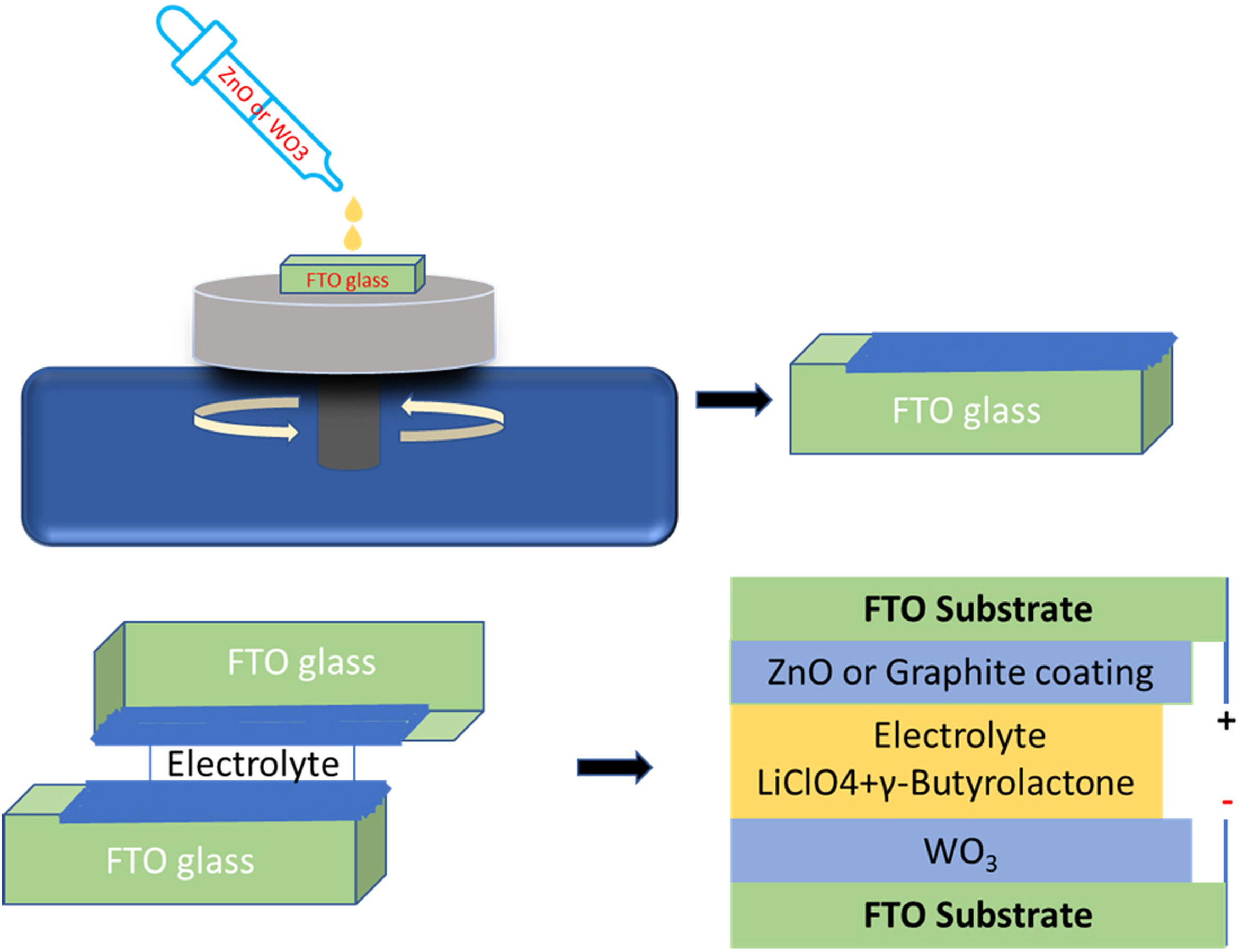
Device assembling procedureFig. 1 shows a schematic representation of the electrochromic device assembly. Two different types of ECDs were prepared, in which the working electrode (WE) of both ECDs was WO3 on FTO and as counter electrode (CE) ZnO coated FTO or C coated FTO. The devices were labeled as ZnO-CE and C-CE, depending on the deposited counter electrode is ZnO or graphite, respectively. The device was assembled as follows. First, the edges of ZnO coated FTO and graphite coated FTO were covered with an insulation tape (Tesa, article no. 56192-10) to obtain a resulting active window of 15mm×15mm. The spacing between the working and counter electrode is 0.20mm.

Then, both counter electrodes were placed on a rigid flat surface. After this, four drops of electrolyte (GBL) were added to the active window of the counter electrode (ZnO or graphite coated FTO), and then the working electrode (WO3 coated FTO) was gently placed on the top in such a way that the conductive sides of the counter and working electrodes were in contact with the electrolyte. Finally, after the elimination of air bubbles, the electrodes were clamped together.
Characterization techniquesThe crystal structure of ZnO-FTO and WO3−–FTO thin films were characterized by X-ray diffractometer (Bruker D8 Advance) equipped with a Cu–K radiation source (λ=0.154nm). The 2θ range was varied between 20° and 70° at a scan speed of 2s/step. Raman spectra were acquired using a Raman spectroscopy system (Horiba Scientific, Xplora Plus) with a 532nm excitation laser at room temperature. The spectral range of 100–1200cm−1 was probed to characterize the sample.
A field emission scanning electron microscope (FE-SEM) coupled with an energy dispersive X-ray spectrometer (EDX) (LEO-Zeiss, Germany) was used to analyze the surface morphologies and textural features of ZnO–FTO and WO3−–FTO thin films. The composition of the thin films was analyzed using X-ray photoelectron spectroscopy (XPS) with a PHI Quantera SXM system. Monochromatic Al Kα radiation (1486.8eV) was used with a spot size of 100μm, a pass energy of 280eV, and a range of 0–1100eV to determine the elemental composition of the sample.
Finally, the EC devices were characterized by UV–Vis spectrophotometer (PerkinElmer Lambda 950) in the wavelength range 400–800nm to study the optical properties. The electrochemical characterization was performed using Multichannel Potentiostat (VMP3 from Biologic, Seyssinet-Pariset, France) to study the stability and operation of the device. CV measurements were performed starting from 0.0V and at the potential range of +4 to −4V at a scan rate of 200mV/s for 20 cycles. CA was performed with positive pulses of +3.5V and negative pulses of −3.5V for 20 cycles. Electrochemical impedance measurements (EIS) were performed using the same potentiostat/galvanostat and measured the open circuit potential (OCP) during 60s before each measurement. EIS spectrum was recorded in the range from 100kHz to 100mHz, with 6 points per decade and amplitude of 10mV versus the OCP. After each measurement the device was cycled using pulse of −3.5V for 20s to obtain tinted state. The device was then left to wait for 5min after which the OCP and EIS measurement was repeated.
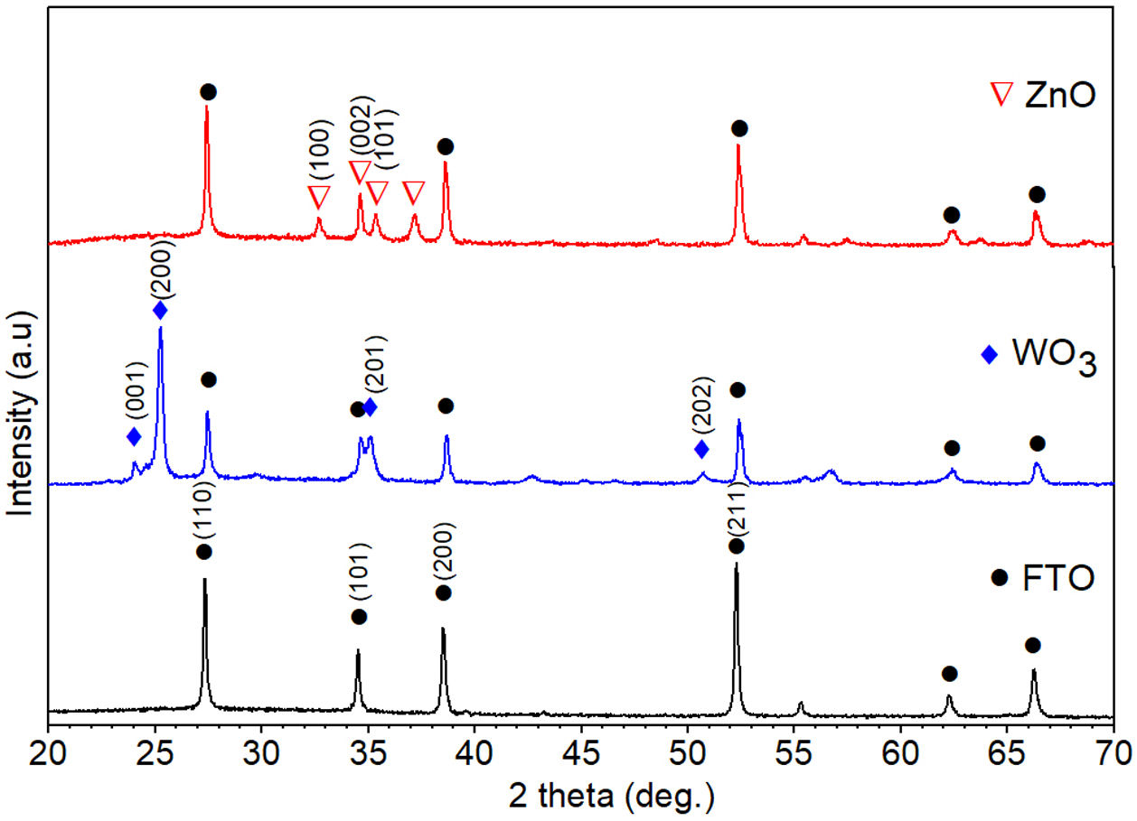
Results and discussionStructural and morphological characterizationThe XRD patterns of FTO glass, ZnO and WO3 thin films deposited on FTO glass substrates annealed at 500°C for 1h are shown in Fig. 2. The diffraction peaks associated with the FTO substrate were identified and indexed with a tetragonal SnO2 phase (JCPDS card no 41-1445). XRD pattern obtained for WO3 film deposited on FTO glass shows diffraction peaks at 2θ angles of 23.9°, 25.2°, 35.1°, and 50.7° associated with a monoclinic crystal structure of WO3 (JCPDS No. 83-0950) [47,48]. Moreover, the diffraction pattern of ZnO thin film shown reflections at 2θ=32.76°, 34.66°, and 35.36°, assigned to (100), (002), and (101) crystallographic planes of ZnO as hexagonal wurtzite structure (JCPDS No. 36-1451). The ZnO film is orientated along (002) plane indicating a wurtzite structure with a preferred c-axis orientation [47,49]. In the X-ray diffraction patterns of WO3 and ZnO films are identified the peaks associated with the FTO substrate. Triton X-100 species are not identified in the XRD pattern of WO3 indicating that the surfactant has been completely removed during calcination and confirming the purity of the sample. The average crystallite size (D) was determined using the Debye–Scherrer equation [50] (Eq. (1)) based on XRD data.
where D is the calculated size of the particle, λ is the X-ray radiation wavelength (λ=1.541Å), θ is the Bragg angle, and β is the full width at half maximum intensity of the respective reflection (FWHM). The average crystallite size of ZnO coated FTO glass was found to be 42.2nm, while the crystallite size of WO3 coated FTO glass was 38.5nm.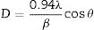
, WO3 (b) and ZnO (c) thin films coated on FTO glass substrates.")
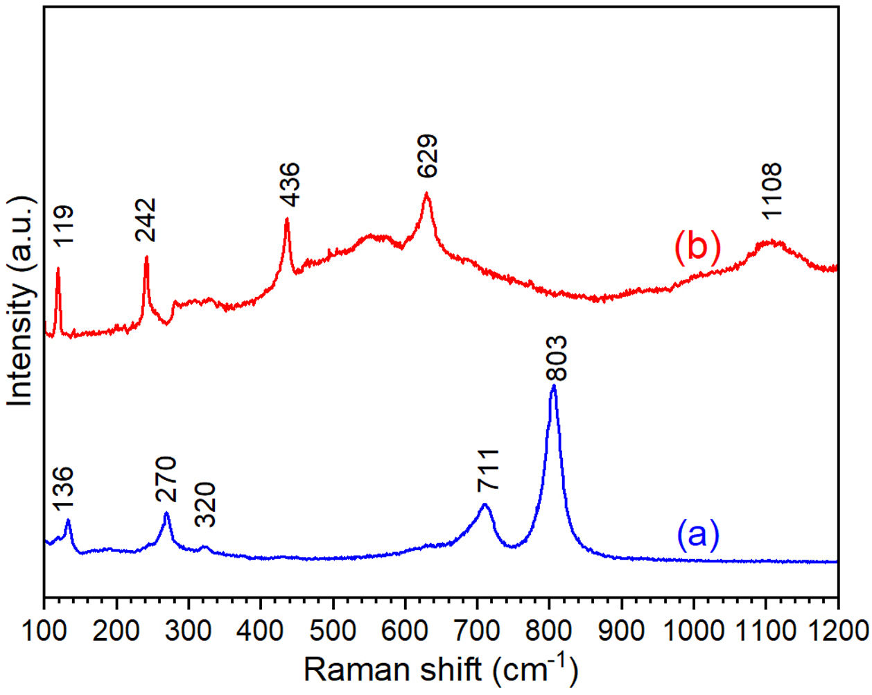
Fig. 3 shows the Raman spectra of the WO3 and ZnO films deposited on FTO substrate. Raman spectrum of WO3 film (Fig. 3(a)) shows well defined peaks at 136, 270, 320, 711 and 803cm−1 associated with the presence of monoclinic WO3. The peaks around 270cm−1 and 320cm−1 can be ascribed to OWO bending mode of bridging oxygen, while the peaks at 711 and 803cm−1 are attributed to WOW stretching mode of WO3. Finally, the peak at 136cm−1 corresponds to the vibrational mode of WO3 monoclinic lattice [51]. In the case of ZnO film, the Raman spectrum shows peaks at 119 and 436cm−1 corresponding to low and high frequency E2 (high) mode in Wurtzite ZnO [52]. The bands at 242, 629 and 1108cm−1 are associated with the FTO substrate [52]. These results are in good agreement with XRD results shown in Fig. 2.
 and ZnO (b) thin films on FTO glass substrates.")
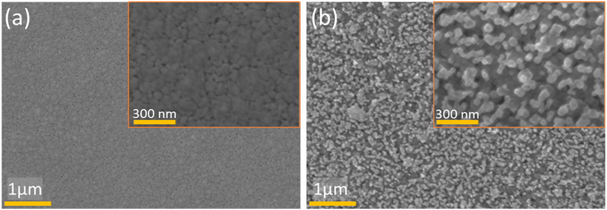
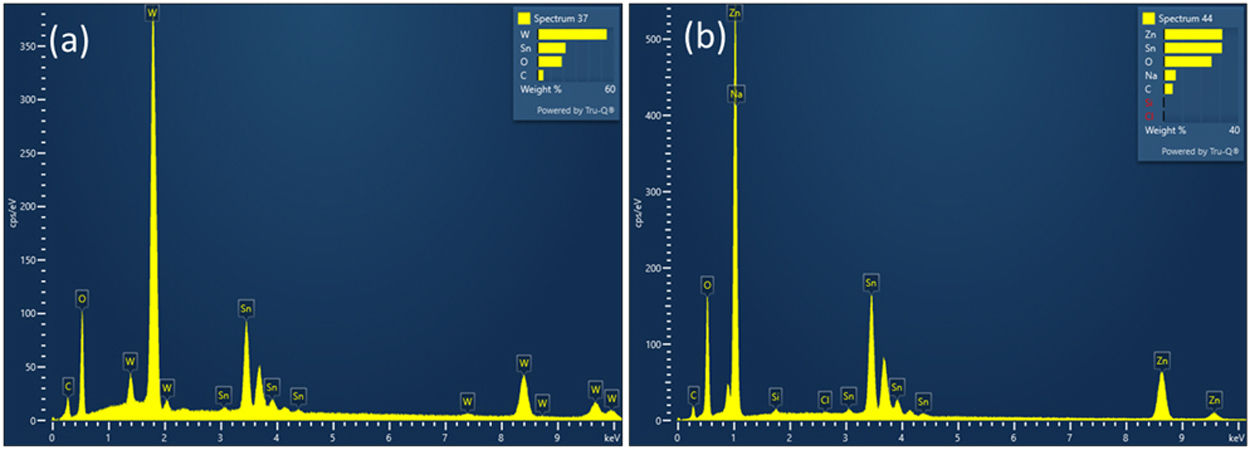
The crystal orientation and microstructural properties of WE and CE layers greatly influence the coloring and bleaching process [15]. Thus, FE-SEM studies of WO3 and ZnO thin films deposited on FTO substrates annealed at 500°C for 1h were performed (Fig. 4). SEM image of the WO3 thin film (Fig. 4(a)) shows a surface with irregular nanoclusters with sizes between 30 and 100nm in diameter, and a nanoporous structure. The porous structure of WO3 can facilitate the migration of lithium ions, and consequently enables coloration change of WO3 film [53]. On the other hand, Fig. 4(b) shows a hexagonal-shaped ZnO nanoparticles growing on FTO substrates. The average diameter of hexagonal crystals was about 30–100nm, showing agglomeration of the particles. The SEM image of ZnO coated FTO shows a more mesoporous structure than the WO3 coated FTO, suggesting a larger surface area and better interaction with the electrolyte compared to graphite coated FTO. The total thickness of ZnO film on FTO glass substrates was found to be approximately 430–450nm, as evidenced by the cross-sectional SEM image shown in Fig. S1 Energy dispersive X-ray (EDX) analysis was performed to evaluate the chemical composition of deposited ZnO and WO3 thin films on FTO glass substrate (Fig. 5). The EDX analysis confirmed the presence of Zn and O elements in the ZnO film (Fig. 5b), and W and O elements in the WO3 film (Fig. 5a). The Sn element is present in both cases and is related to substrate FTO.
 and ZnO (b) thin films coated on the FTO glass substrates.")
 and ZnO (b) thin films coated on the FTO glass substrates.")
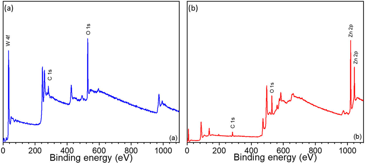
In addition to EDX analysis, X-ray photoelectron spectroscopy (XPS) was also used to obtain more information about the surface elemental composition of WO3 and ZnO thin films and to identify the present chemical species. Binding energy (Ev) of WO3 and ZnO thin films in the range from 0 to 1100eV was determined by the qualitative XPS survey scan. Fig. 6 shows the XPS spectra of the WO3 and ZnO thin films deposited on FTO glass and annealed at 500°C [54,55]. The appearance of W 4f, Zn 2p and O 1s peaks confirm the composition of films and the presence of WO3 and ZnO, respectively (Fig. 6a and b). A weak C 1s peak at 284eV was also observed and associated with carbon-containing molecules adsorbed onto the film surface.
Optical, electrochemical, and electrochromic properties and ZnO (b) thin films coated on the FTO glass substrates.")
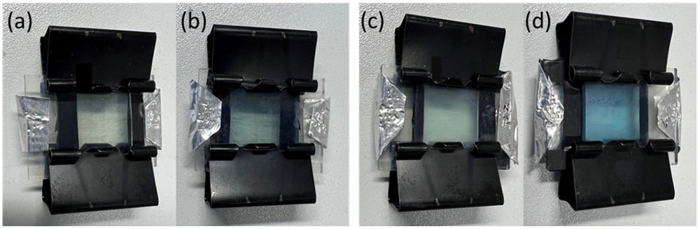
Fig. 7(a–d) shows the bleached and colored states of the EC devices for applied voltages of −2.5V for coloration and +2.5V for bleaching. The color of the C-CE and ZnO-CE based ECDs changes from transparent (bleached state) to blue (colored state). However, the intensity of coloration is much higher and visible in ZnO-CE (Fig. 7c, d) than in C-CE based ECD (Fig. 7a, b).
 and ZnO-CE (c, d) based ECDs.")
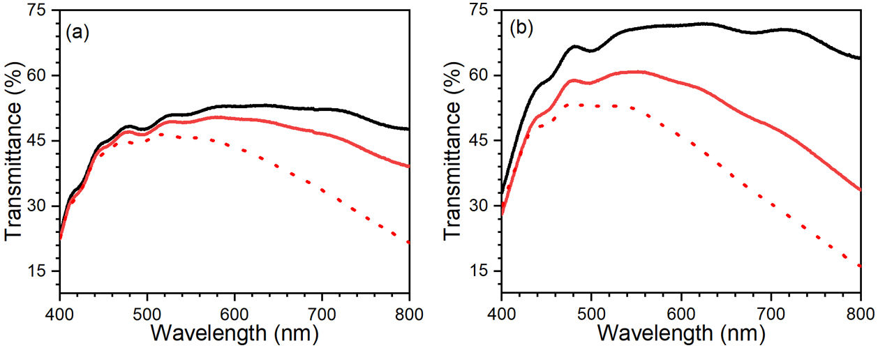
Following the assembling procedure of the ECDs (explained in “device assembling procedure” section), the difference in transmittance between colored and bleached states was determined in the wavelength range of 400–800nm (Fig. 8). As seen in Fig. 8, the transmittance variation is also quite different for both devices in bleached and colored states. Fig. 8 shows a substantial decrease in transmittance under the bleached condition, attributed to reflection at the conducting glass electrodes [56]. The transmittance of FTO, graphite layer on FTO, 5-layers of WO3 on FTO, 3-layers of ZnO on FTO were also provided in Fig. S2. Before potential was applied, the initial state of the ECD has higher transmittance due to the absence of electrochromic reactions. However, during the ECD cycle, ion diffusion and intercalation processes were observed within the WE and CE electrodes [57]. Differences in transmittance and cathodic coloring at 445 and 435nm were observed for C-CE and ZnO-CE EC devices, respectively. In particular, a considerable difference in the transmittance of bleached and colored states was observed in the visible–NIR spectrum (∼440–800nm) for ZnO-CE based ECD (Fig. 8(b)), associated with the higher transparency of ZnO thin films on FTO glass and indicating that the ZnO-CE device had better electrochromic properties than the C-CE [58,59].
 and ZnO-CE (b) based ECDs. The bleached state shown in red line and tinted state shown in dotted red line. Black line represents without applying potential.")
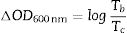
Coloration efficiency (η), defined as the change in optical density (OD) per unit of charge (Q) intercalated or deintercalated from the EC, is the most critical parameter to obtain a comprehensive evaluation of ECDs. A high (η) indicates a device that offers a large optical contrast. The η can be calculated from Eqs. (2) and (3):
where ΔOD is change in optical density at 600nm, Tb and Tc represent the transmittance in bleached and colored states of the film at a certain wavelength, respectively and Q is the charge density per unit area. The changes in ECD transmittance at 600nm were used to determine change in optical density. A transmittance modulation of 6.5% was observed for C-CE and 12.4% for ZnO-CE. The calculated η value of ZnO-CE and C-CE devices was 41.6 and 19.8cm2C−1, respectively, similar to previously reported values [60–63].
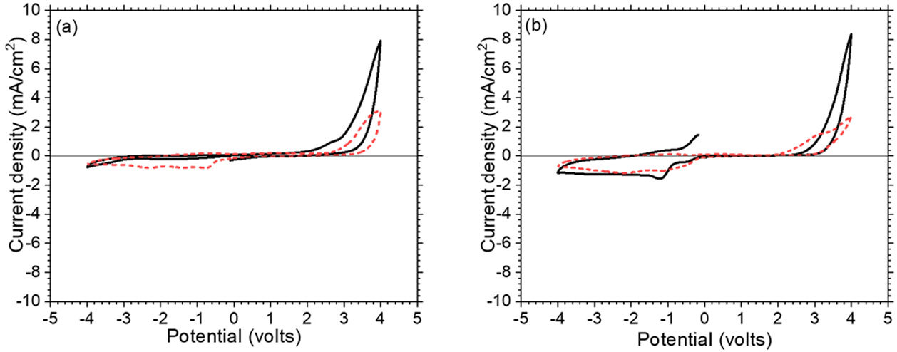
The electrochemical analysis provides information on the cathodic and anodic behavior of ZnO-CE and C-CE devices. To carry out the analysis the cyclic volatmetry (CV) and chronoamperometry measurements were performed (Figs. 9 and 10). In general, a gradual increase in the intensity of blue coloration is observed for WO3-Zn and WO3-C devices as the result of cathodic polarization [57]. The optical changes involve redox processes in ZnO-CE and C-CE devices at the interface of electrodes accompanying the Li+ ions insertion to the surface of the WO3 thin film from the electrolyte. In the case of C-CE (Fig. 9(a)) and ZnO-CE (Fig. 9(b)) ECDs, the potential decreased during the cathodic scan, and at the potential of −4.0V corresponded to deep blue coloration. At this point, W6+ was reduced to W5+. The coloring occurs due to a rapid reduction reaction in the WO3 film involving Li+ insertion. An oxidation reaction with equivalent charge takes place at the CE (C or ZnO) surface to compensate for the current at the WO3 film. In the case of ZnO-CE, a reduction peak was observed at around −1.1V, which could be due to the side reaction of ZnO with H2O at the beginning of the experiment. After several cycles, the peak was gradually disappeared, suggesting that the water content had reacted completely with the Zn-OH hydroxyl groups, since no visible bubbles were observed that would suggest breakage of water into hydrogen and oxygen gas. In C-CE based ECD such peak was not observed.
 and ZnO-CE (b) based ECDs. 1st cycle is shown in black line and 20th cycle is shown in dotted red line.")
 and C-CE (b) for first 2 cylces. Charging and discharging are shown in black and red color respectively.")
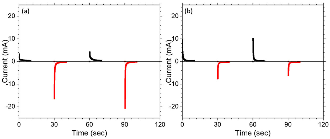
CA was performed to investigate the response time which is the measure of speed in which electrochromic device change between a colored state and a bleached state. Fig. 10(a, b) shows chronoamperograms of the assembled C-CE and ZnO-CE based devices for the first 2 cycles recorded at ±3.5V with a time interval of 20s. In Fig. 10, the current drawn for the coloring is higher in the case of C-CE based ECD (6.9mAs) than that for ZnO-CE based ECD (5.6mAs), for the first cycle. However, the current consumed to discharge Li+ for ZnO-CE is higher [64]. It was recently reported that constructing a heterostructure for electrode materials may be a useful way to accelerate charge transportation [65].
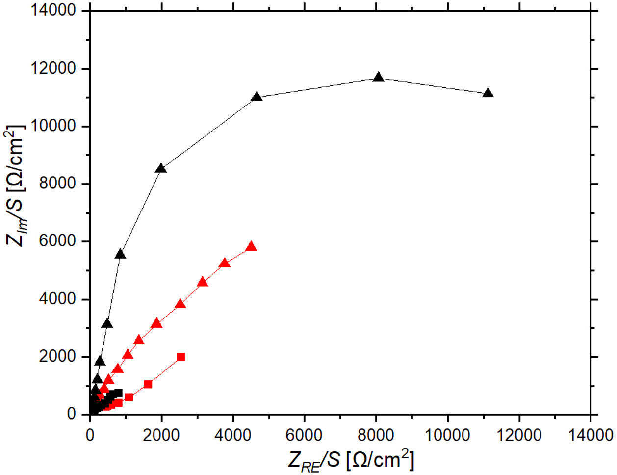
Electrochemical impedance spectroscopy tests were performed to understand the charge transfer and ion diffusion processes that occur at the coated electrode surface as well as to gain insight into the mechanism driving the electrochromic behavior. Fig. 11 shows a Nyquist plot of ZnO-CE and C-CE based devices measured in the frequency region from 0.1Hz to 100kHz. The Bode plot illustrating the change in magnitude |Z| and phase angle as a function of frequency, Hz, for both the bleached and tinted states of the tested ECDs (Fig. S3 of the supplementary file). The semi-circle in the Nyquist plot indicates a capacitive behavior of the electrochromic device, which is caused by the capacitance of the double layer formed at the interface between the working electrode and the electrolyte [66]. For both EDCs, there are changes in impedance during the tinting and bleaching cycles. This indicates that there is a consistent change between the bleached and tinted state, which is likely related to Li+ intercalation and deintercalation. Specifically for C-CE device, the impedance shifts between relatively high impedance (Z) achieving over 5kΩ for tinted state and then drops below 3kΩ in bleached state. With the replacement of carbon electrode with ZnO, the difference between bleached and tinted states is more present. This change in impedance is likely due to changes in the concentration of Li+ ions in the electrolyte and changes in the saturation of Li+ ions in the nanopores of WO3 thin film as it intercalates or deintercalates from crystal lattice [14]. In the device where ZnO is used as a counter electrode, the change in impedance observed in the Nyquist plot could be attributed to the intercalation and deintercalation of Li+ ions, which results in changes in the surface of ZnO, such as the formation of ZnOH or other surface modifications [67]. The visual observations and recorded transmittance spectra suggest that the Li+ ions are being more effectively intercalated into the WO3 layer, affecting also to the surface of ZnO [67,68].
Conclusions and ZnO-CE (black) based devices representing the tinted (triangles) and bleached (squares) state after an applied potential.")
Cost-effective and simple sol–gel method was used for the preparation of transparent stable WO3 and ZnO layers on FTO substrates by spin-coating. ECDs were successfully assembled using WO3 thin film as WE and ZnO thin film or graphite as CE, and a LiClO4-GBL solution as the electrolyte. XRD results confirm the crystallization of monoclinic WO3 and hexagonal wurtzite (ZnO) phases after annealing at 500°C/1h. Under operative conditions, the ZnO film, used as a counter electrode, improves the coloration efficiency of ECD and almost doubles it compared to a graphite electrode. The higher optical contrast and coloration efficiency of ZnO-CE compared to C-CE ECDs are attributed to its high active specific surface area of ZnO nanoparticle coating. Thin films of ZnO as CE are compatible with WO3-based electrochromic devices, obtaining higher coloration efficiency and better transparency of the device in bleached state. This indicates that ZnO thin films would be an efficient replacement for existing platinum and graphite thin film deposits and could influence the development of novel EC technologies.
Since the studied device configuration uses a simple process of fabrication of the EC film, the ZnO-CE based ECD has a great potential for fabrication of large-area and practical electrochromic smart windows for greenhouse covers, electrochromic apertures and smart windows.
This work is a part of the activities of the FunGlass project. This project has received funding from the European Union Horizon 2020 Research and Innovation Program under Grant 739566. This work was also supported by the Grant VEGA 1/0844/21 of the Grant Agency of the Slovak Republic and the authors are grateful to the JECS Trust for funding (contract No. 2022301).
The following are the supplementary data to this article: