


Silicon carbide-based composite ceramic is manufactured by one-stage selective laser sintering. The effect of the sintering parameters and raw materials on the sinterability of SiC based composite is studied. The optimization of the parameters is carried out. In a single stage of selective laser sintering, it is possible to achieve 87% relative density. The influence of particle size of feedstock, as well as BN and Y2O3 additives on the sinterability, mechanical and thermal properties of the samples are studied.
For composites that contain 10% BN, the thermal expansion coefficient increases from room temperature to 900°C. The electrical resistivity decreases both in the room and at cryogenic temperature (−200°C). The thermal conductivity and mechanical properties of BN-containing samples decrease as well. Yttrium oxide-containing samples show higher thermal conductivity and electrical resistivity than boron nitride-containing samples.
Composites basados en carburo de silicio (SiC) han sido procesados en un solo paso mediante fusión selectiva por láser (SLS). El efecto de los parámetros de procesado por SLS en la sinterización de los composites basados en carburo de silicio ha sido estudiado y se ha llevado a cabo su optimización. Mediante la fusión selectiva por láser, sin emplear postratamientos, se han conseguido densidades relativas del 87%. Se ha evaluado la influencia de la incorporación de aditivos como el nitruro de boro (BN) y el óxido de itrio (Y2O3) en la sinterización y las propiedades mecánicas y térmicas.
Para composites a los que se ha incorporado un 10% en peso de BN, la resistividad eléctrica disminuye a temperatura ambiente y a bajas temperaturas (−200°C). La conductividad térmica y las propiedades mecánicas disminuyen en las muestras que contienen BN. Por otra parte, la incorporación de óxido de itrio aumenta la conductividad térmica y la resistividad eléctrica en comparación con las muestras que contienen BN.
The development of powerful devices and miniaturization of electronics in the last decades have implied an increase in the power density of electronics. New requirements push scientists and engineers develop ever-improving materials, tools, processes, and design methodologies [1,2]. Decreasing the size and increasing the power of transistors and other integrated circuit devices over time have enhanced computing capabilities at the cost of increased power dissipation across the device, and system levels [3]. The power required for high-performance computing applications on some processor modules can reach up to 250W or more generating heat loads of around 1kW for the processors alone in a four-socket computing system [4].
It is expected that heat flux levels soon may exceed 100W/cm2 for commercial electronics and over 1000W/cm2 for selected high power [5]. There is also a growing demand for more sophisticated and capable electronics used in harsh environment applications such as those found in defense, air space, automotive, and oil exploration systems. Thermal management of harsh environment electronics is vital to the successful design, manufacture, and operation of a different electronic system to meet the high/cryogenic temperature, environmental, reliability, and cost-effectiveness requirements.
To address the challenge linked with high-efficiency thermal management systems there are mainly two approaches including (i) new materials with higher thermal conductivity, and (ii) improving the design of thermal management systems. To meet all of those criteria new and highly adapted designs and materials must be used.
Ceramic materials for thermal management systemsCeramic-based materials are used for thermal management in space applications. The main advantage of ceramic material is their low thermal expansion coefficient, excellent mechanical properties, corrosion and erosion resistance, dielectric properties, and chemical stability. However, ceramics usually have low thermal conductivity.
Commonly used ceramics with thermal conductivity are AlN, SiC, and BeO [6]. They are mainly used in assembling power components. Beryllium oxide has a very high thermal conductivity. However, it is toxic. Aluminum nitride and silicon carbide are good candidate materials as they have low thermal expansion coefficient, which matches well with silicon [7]. However, both of them are difficult to sinter because of their highly covalent and low diffusive nature [8].
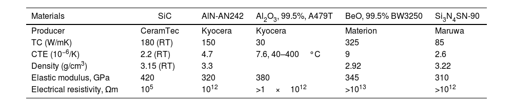
In Table 1.1, common materials for the Thermal Management System (TMS) and their properties are summarized. Table 1.2 depicts the commercially available ceramic materials and their properties. The practical outcome of those tables is the numerical values of the key parameters. Any new material to be used for TMS must possess better characteristics (both material and process viewpoints) compare to the existing and commercialized products.
Materials for a TMS and their properties.
| Materials | SiC | AlN-AN242 | Al2O3, 99.5%, A479T | BeO, 99.5% BW3250 | Si3N4SN-90 |
|---|---|---|---|---|---|
| Producer | CeramTec | Kyocera | Kyocera | Materion | Maruwa |
| TC (W/mK) | 180 (RT) | 150 | 30 | 325 | 85 |
| CTE (10−6/K) | 2.2 (RT) | 4.7 | 7.6, 40–400°C | 9 | 2.6 |
| Density (g/cm3) | 3.15 (RT) | 3.3 | 2.92 | 3.22 | |
| Elastic modulus, GPa | 420 | 320 | 380 | 345 | 310 |
| Electrical resistivity, Ωm | 105 | 1012 | >1×10¹² | >1013 | >1012 |
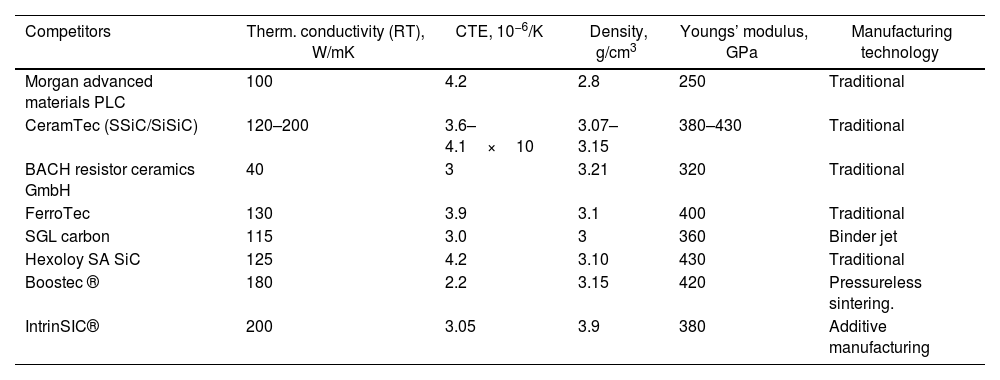
Overview on properties of used materials for TMS.
| Competitors | Therm. conductivity (RT), W/mK | CTE, 10−6/K | Density, g/cm3 | Youngs’ modulus, GPa | Manufacturing technology |
|---|---|---|---|---|---|
| Morgan advanced materials PLC | 100 | 4.2 | 2.8 | 250 | Traditional |
| CeramTec (SSiC/SiSiC) | 120–200 | 3.6–4.1×10 | 3.07–3.15 | 380–430 | Traditional |
| BACH resistor ceramics GmbH | 40 | 3 | 3.21 | 320 | Traditional |
| FerroTec | 130 | 3.9 | 3.1 | 400 | Traditional |
| SGL carbon | 115 | 3.0 | 3 | 360 | Binder jet |
| Hexoloy SA SiC | 125 | 4.2 | 3.10 | 430 | Traditional |
| Boostec ® | 180 | 2.2 | 3.15 | 420 | Pressureless sintering. |
| IntrinSIC® | 200 | 3.05 | 3.9 | 380 | Additive manufacturing |
Silicon carbide is considered to have a high potential to fulfill strict requirements of the space industry and is applied as a high thermal conductive material. Silicon carbide has one of the highest thermal conductivity (TC), and lowest coefficient of thermal expansion (CTE). It is lightweight compared with other ceramics used in thermal management systems. However, silicon carbide did not get a wide application in TMS because of several challenges;
- (i)
SiC requires high sintering temperatures [9]. In the early 1970s, it was reported that β-SiC powders can be sintered to high densities at a very high temperature of about 2100°C [10]. Next, it was manifested also that α-SiC powders are sinterable under similar conditions [11].To sinter SiC powder in relatively lower temperatures e.g., 1800–2000°C is needed to add sintering additives, which influences the properties of SiC [12]. This is especially challenging when SiC should be integrated with materials with low temperatures.
- (ii)
Silicon carbide has low electrical resistivity [13]. Often TMS is integrated with the conductive layers of the vehicles, where high electrical resistivity (or dielectric constant) is needed. The resistivity value of pure SiC is in the order of 105Ωm. Some sintering additives enable to achieve higher electrical resistivity, but they drastically influence TC.
- (iii)
The traditional manufacturing methods of SiC have limitations in terms of design. Therefore, SiC-based TMS is not applied for the fabrication of parts having complex designs. For example, the application of SiC in packages is strongly limited.
The consolidation of SiC and SiC based composites are mainly fulfilled by a sintering process. Sintering can be both with or without applied pressure. The solid-state sintering usually happens at high temperatures and high-pressure atmospheres. Traditionally, silicon carbide-based parts are made by high temperature co-fired ceramics (HTCC), Low temperature co-fired ceramic (LTCC) [14], pressure-less and hot pressure sintering [15,16], hot isostatic pressing sintering (HIP) [17], reaction sintering [18,19] methods. Each of these manufacturing technologies has its unique advantages. However, these technologies are multistage and resource-consuming.
The development of single loop architectures with more advanced geometries could save significant weight, reduce system complexity, and increase the reliability of functional parts. It must be underlined also that some complex designs are not possible to achieve by traditional processing methods.
The solution to those challenges can be Additive Manufacturing (AM) which is a promising method to achieve more advanced designs with fewer geometric limitations [20].
Additive manufacturing (AM) also called 3D printing is the building of a three-dimensional object from a CAD model or a digital 3D model [21]. This approach enables design flexibility and consumes fewer resources (energy and toxic chemicals) compare to the traditional processing methods. Using the AM for fabrication of the parts and articles constructed on SiC-based composite would be great added value in the technological chain. The AM will significantly decrease material consumption, process time, and cost [22].
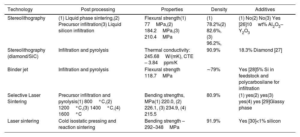
There are attempts to manufacture silicon carbide-based ceramic using both direct and indirect AM technology [23]. Polymer-based slurries are prepared for AM by stereolithography and direct ink writing [24]. Those processes are followed by polymer pyrolysis to obtain densified SiC. However, in most cases, the final products are contaminated by residual polymer or its by-products. This negatively influences the target properties and device performance. Successful technology for manufacturing SiC-based composite is the binder jet [25], which is used to prepare commercial parts with various functionality. Promising achievements are recorded laser sintering technology. In Table 1.3 the AM technologies for fabrication of the SiC and its properties are summarized [26–30].
AM fabrication of SiC and its properties.
| Technology | Post processing | Properties | Density | Additives |
|---|---|---|---|---|
| Stereolithography | (1) Liquid phase sintering,(2) Precursor infiltration(3) Liquid silicon infiltration | Flexural strength(1) 77MPa,(2) 184.2MPa,(3) 210.4MPa | (1) 78.2%(2) 82.6%,(3) 96.2%, | (1) No(2) No(3) Yes [26]10wt% Al2O3–Y2O3 |
| Stereolithography (diamond/SiC) | Infiltration and pyrolysis | Thermal conductivity: 245.68W/(mK), CTE – 3.84ppm/K | 90.9% | 18.3% Diamond [27] |
| Binder jet | Infiltration and pyrolysis | Flexural strength 118.7MPa | ∼79% | Yes [28]5% Si in feedstock and polycarbosilane for infiltration |
| Selective Laser Sintering | Precursor infiltration and pyrolysis(1) 800°C,(2) 1200°C,(3) 1400°C,(4) 1600°C | Bending strengths, MPa(1) 220.0, (2) 226.1, (3) 234.9, (4) 215.5 | 80.9% | (1) yes(2) yes(3) yes(4) yes [29]Glassy phase |
| Laser sintering | Cold isostatic pressing and reaction sintering | Bending strength – 292–348MPa | 91.9% | Yes [30]<1% silicon |
It is clear that the AM could be the best solution for the fabrication of SiC based TMS with complex shapes and geometry. Moreover, the process is low energy and time-consuming, thus it has huge potential to improve the TMS's design and performance.
However, AM also has some challenges to be solved. Particularly, the development of raw material for AM feedstock is still an issue and huge efforts have been dedicated to finding suitable feedstock compositions for AM.
The main goal of this work is twofold (i) to develop the composition of raw material for AM of SiC based parts with predefined shapes and properties. Here, the ultimate goal is also to use functional additives and control physical parameters of the final product, (ii) to develop and optimize the process for fabrication SiC based vehicles.
Materials and methodsFeedstock preparationThe feedstock containing SiC, Si, and additives was prepared using a dry mixing approach, i.e., using a planetary ball miller. Firstly, two different powders were weighed and added to the jar. Zirconia balls of 10mm in diameter were added to the zirconia jar. The ratio of the powder to the ball was 3:1 by the weight. The jar was placed into the planetary miller and rotated for 2h with 20r/min.
To fine-tune and control feedstocks’ parameters such as flowability and sinterability as two main parameters have been modified and the outcomes were monitored. The first parameter was the composition of the raw material, and the second parameter was the particle size distribution. The main goal of those changes was to estimate the best combination of raw materials to achieve good flowability and sinterability of the feedstock. In addition to those main 2 parameters, the effect of additives on the properties of samples was estimated as well.
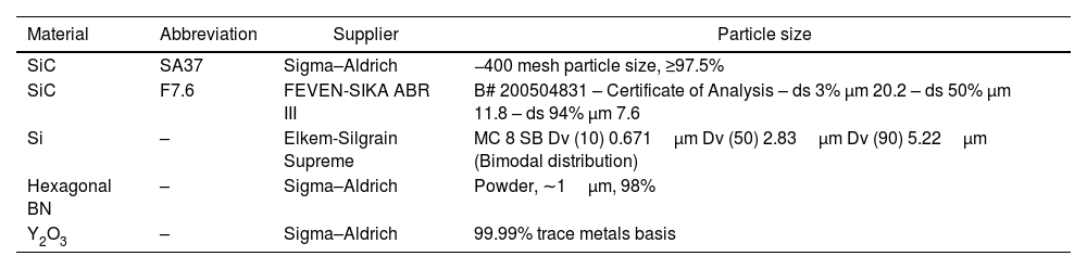
The precursors and their suppliers are summarized in Table 2.1.
Precursors purchased from different suppliers.
| Material | Abbreviation | Supplier | Particle size |
|---|---|---|---|
| SiC | SA37 | Sigma–Aldrich | −400 mesh particle size, ≥97.5% |
| SiC | F7.6 | FEVEN-SIKA ABR III | B# 200504831 – Certificate of Analysis – ds 3% μm 20.2 – ds 50% μm 11.8 – ds 94% μm 7.6 |
| Si | – | Elkem-Silgrain Supreme | MC 8 SB Dv (10) 0.671μm Dv (50) 2.83μm Dv (90) 5.22μm (Bimodal distribution) |
| Hexagonal BN | – | Sigma–Aldrich | Powder, ∼1μm, 98% |
| Y2O3 | – | Sigma–Aldrich | 99.99% trace metals basis |
To optimize the feedstock composition and estimate the effect of additives, the main components were mixed in different ratios and required additives were added. The purpose of adding an additive was to fine-tune sinterability and control the physical properties of the end products.
Apart from the composition, the particle size and distribution play a key role in the additive manufacturing process: hence in this study, we explored the effect of the particle size, too. We selected two types of silicone carbide (a) relatively large particle size with an average 37μm particle size (SA37) (b) small particle size with an average particle size of 7.6μm (F7.6).
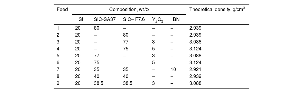
In Table 2.2 the compositions of the feedstocks used in this study are summarized.
Composition of feedstock.
| Feed | Composition, wt.% | Theoretical density, g/cm3 | ||||
|---|---|---|---|---|---|---|
| Si | SiC-SA37 | SiC– F7.6 | Y2O3 | BN | ||
| 1 | 20 | 80 | – | – | – | 2.939 |
| 2 | 20 | – | 80 | – | – | 2.939 |
| 3 | 20 | – | 77 | 3 | – | 3.088 |
| 4 | 20 | – | 75 | 5 | – | 3.124 |
| 5 | 20 | 77 | – | 3 | – | 3.088 |
| 6 | 20 | 75 | – | 5 | – | 3.124 |
| 7 | 20 | 35 | 35 | – | 10 | 2.921 |
| 8 | 20 | 40 | 40 | – | – | 2.939 |
| 9 | 20 | 38.5 | 38.5 | 3 | – | 3.088 |
The 7th column in Table 2.2 is the calculated theoretical density of the composite. This was calculated by considering the amount of each component and its theoretical density. The ultimate goal was to achieve as close as possible to those values.
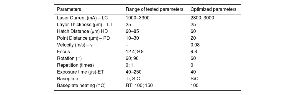
Selective laser sinteringSintering of the powder was performed by Selective Laser Melting (SLM) technique using a Metal 3D printer (Realizer GmbH SLM-50, Germany). During the sintering, the chamber was sealed with a high-purity Argon gas (>99.9vol.%) to avoid oxidation and degradation of the powder. The focused laser beam (IPQ Laser GmbH, YLM-120-AC, 120W, YAG: Nd3+ with 1.06μm wavelength) was then directed onto the powder bed to form the pattern according to CAD design. The laser beam is deflected by Galvano mirrors, which control the movement of the laser source over the surface of the powder bed. The powder was spread by a wiper over the surface of a 50mm×50mm×5mm (length×width×depth) Silicon Carbide platform. In each layer, the laser beam followed a prescribed scanning path. Solidification was obtained by (partly) fusing or sintering selected areas of the successive powder layers using thermal energy supplied through a laser beam. When a layer is scanned, the build cylinder moves down one step – typically 25μm (layer thickness), and the wiper spread the next layer of powder. The process was repeated until the manufacturing of the designed part was completed. The laser current was altered from 1000 to 3300mA (Table 2.3).
Set of parameters applied for optimization of SLM process.
| Parameters | Range of tested parameters | Optimized parameters |
|---|---|---|
| Laser Current (mA) – LC | 1000–3300 | 2800, 3000 |
| Layer Thickness (μm) – LT | 25 | 25 |
| Hatch Distance (μm) HD | 60–85 | 60 |
| Point Distance (μm) – PD | 10–30 | 20 |
| Velocity (m/s) – v | – | 0.08 |
| Focus | 12.4; 9.8 | 9.8 |
| Rotation (°) | 60; 90 | 60 |
| Repetition (times) | 0; 1 | 0 |
| Exposure time (μs)-ET | 40–250 | 40 |
| Baseplate | Ti, SiC | SiC |
| Baseplate heating (°C) | RT; 100; 150 | 100 |
The bulk density of the SLS-ed samples was measured using the Archimedes method (Mettler Toledo ME204, Greifensee, Switzerland). The samples were immersed in distilled water. The theoretical density of the mixture was calculated using the rule of mixture. Phase characterization was accomplished by Mini Flex 600 X-ray diffractometer, Rigaku (40mA, 40kV, Cu Kα radiation, λ=0.1542nm, step size of 0.02°) for both powders and SLS-ed samples. Microstructural characterization was performed by scanning electron microscope (SEM, Prisma E, Thermo Fisher Scientific, Hillsboro, OR, USA) equipped with an EDS detector. Samples were subjected to coating using a thin layer of Au to provide sufficient conductivity.
Thermal conductivityThermal conductivity was measured using the Transient Plane Source (TPS) (TPS 2500 S, Hot Disk AB, Sweden) method with a sensor element in the shape of a double spiral. This TPS sensor acts both as a heat source for increasing the temperature of the sample and a “resistance thermometer” for recording the time-dependent temperature increase.
Hot Disk sensors with Kapton insulation are used. The Hot Disk sensors are designed to be placed between the plane surfaces of two sample pieces of the samples. Considering the material in our case a material based on SiC, the sizes of the samples are 15±2mm in thickness and a diameter or width of 40±0.2mm.
Electrical propertiesVolume electrical resistivity of the SLS-ed samples was measured using a Chauvin Arnoux C. A series megohmmeter or a test setup consisting of a combination of dedicated laboratory equipment, including an adjustable DC voltage supply, DC voltmeter, and DC combined milli- and micro ammeter. In the former case, the resistance value is directly retrieved from the instrument display; in the latter c+ase, the resistance is calculated based on voltage and current. In the case of using the megohmmeter, the test voltage is varied in the range from 50V to 1000V (chosen such that the test current does not rise to an unsuitably high level, this is determined by the measurement device automatically; the megohmmeter is unable to measure resistances below approximately 30kΩ). In the case of using the DC supply, voltage values were chosen generally to be either 10V or 30V, or lower, in the case of test samples with a smaller resistivity, to avoid heating the test samples with excessive current. The samples are rectangular in shape with 10mm×10mm×5mm.
Thermal expansion coefficientThermal expansion coefficient (CTE) was measured by dilatometer (Netzsch dilatometer DIL 402C). It determines dimensional changes versus temperature or time while the sample undergoes a controlled temperature program. The degree of expansion divided by the change in temperature is called the material's coefficient of expansion (α), where
α-coefficient of expansion, L0 – initial sample length, ΔT – change in temperature, Δl – change in length. For preparing a dilatometer measurement, a prismatic-shaped sample is inserted into a sample holder and brought into contact with the pushrod. After closing the furnace, the experiment can be started. The thermal expansion of the sample during heating, cooling, or under isothermal conditions is detected by the displacement system.Mechanical properties
The compressive test was performed using a computer control universal testing machine (Jinan Zhongchuang Industrial Test Systems Co., Ltd, China). Rectangular samples with a size of 10mm×10mm×5mm were placed between grips and compressive with a 0.5mm/min shear rate. This low rate was selected to be able to follow all transformations in the sample when it was being strained (compressed). Young's modulus was extracted from the slope of the strain–stress curve. The maximum load was estimated to be the point when the samples fully collapsed.
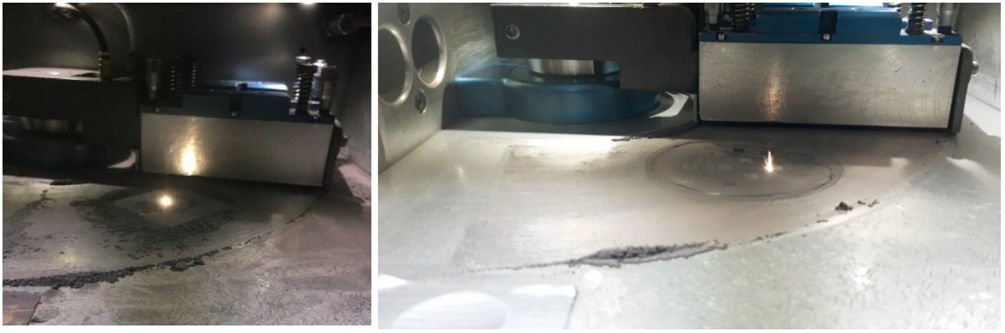
Results and discussionFeedstock preparationPowder flowability is a key parameter greatly influencing the powder bed density, which in its turn affects the sintered parts’ quality including density, roughness, etc. Powder particle shape and size as well as particle size distribution play an important role in sintering kinetics and powder bed formation. For example, the spherical particles of the narrow size distribution have better flowability as compared to the angularly shaped powders. In Fig. 3.1 two extreme cases of flowability are depicted. When the feedstock flowability was insufficient printing process was terminated (Fig. 3.1 left), while good flowability case the printing process was successfully completed (Fig. 3.1 right). The flowability is evaluated visually. When the wiper evens the powder in the chamber, the surface of powder which has bad flowability stays uneven, and accumulation of powder is observed.
 and good (right) flowability.")
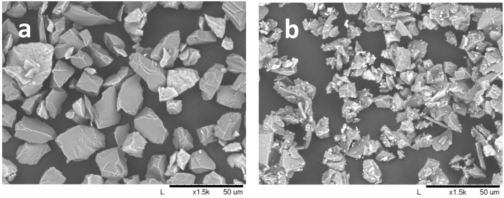
Considering this important factor, we performed microstructural analyses of the raw material. The results are depicted in Fig. 3.2.
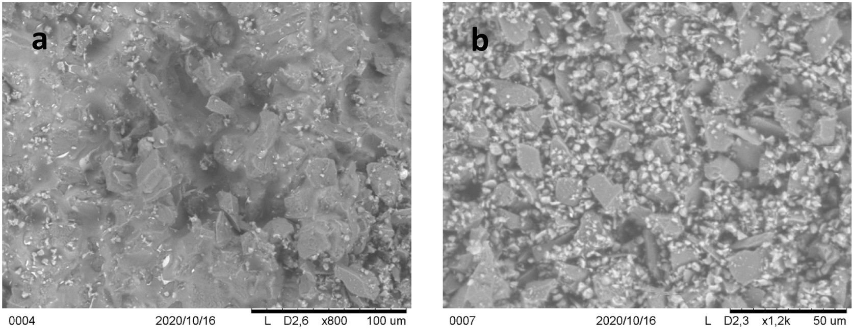
 20% Si–80%SiC (SiC-SA37, Feed 1), (b) 20% Si–80%SiC (SiC– F7.6, Feed 2).")
Microstructural analysis shows that there are particles in the 10 to 50μm range in Feed 1 (Fig. 3.2a) which is a mixture of SiC37 with 400 mesh particle size and Silicon with 10–30μm (Table 2.2). As mentioned above the feedstocks were prepared by dry milling process. It could be the reason for particle size change i.e., reduction. However, before and after milling it was estimated that there was no notable particle size reduction and the milling process did not influence the particle size and shape of the components.
The mixture of Feed 2 consists of SiC7.6 with an average particle size of 7.6μ and Silicon with 10–30μm (Table 2.2).
Selective laser sintering: the effect of the baseplateIt is common knowledge that parameters of laser printing including laser power, scanning speed, hatch spacing, and layer thickness have a high impact on the sintering process, microstructural features, and mechanical properties of the final part. The process parameters may vary from powder to powder; therefore, they should be optimized and the effect of each process parameter on the features/characteristics should be evaluated.
The material of the baseplate also has a notable effect on the sinterability. When titanium baseplates were used, the sintered powder didn’t stick to the baseplate. In Fig. 3.3, the difference in the microstructure of the SLS-ed SiC-based composites on the titanium and SiC baseplates is illustrated. It is seen that in the case of SiC baseplate the particles are more fused while in the case of the metallic baseplate the separate particles in the matrix still are visible. It is hypothesized that the reason is the large difference between thermal expansion coefficients (CTE). Thus, the CTE of SiC is 2.2×10⁻⁶/K, while CTE of Ti64 alloy is 8.6×10⁻⁶/K at room temperature. Such thermal expansion mismatch causes residual stresses, which have a critical effect especially when the heating rate of materials is high. On the other hand, titanium reacts with both silicon and silicon carbide. The reaction is exothermic and can lead to a sharp increase of temperature in the sintering micro zone, which itself can lead to evaporation of the rest of the silicon and at the same time generate thermal residual stresses. These stresses can contribute to crack formation in the interface of those two materials, which results in the detachment of the samples from baseplates. Additionally, titanium reaction with silicon and/or silicon carbide forms brittle silicide phases (such as Ti5Si3, TiSi2). Ti5Si3 has high thermal expansion anisotropy (αc/αa≅2.7) due to the large difference in the thermal expansion coefficients along the (5.98×10⁻⁶K−1) and c (16.64×10⁻⁶K−1) axes and can cause microcracks during fast heating and cooling [31]. However, to better understand the reason for such behavior, a deep research study is ongoing.
Influence of the laser current on the sintering process SiC baseplate, (b) Ti64 baseplate.")
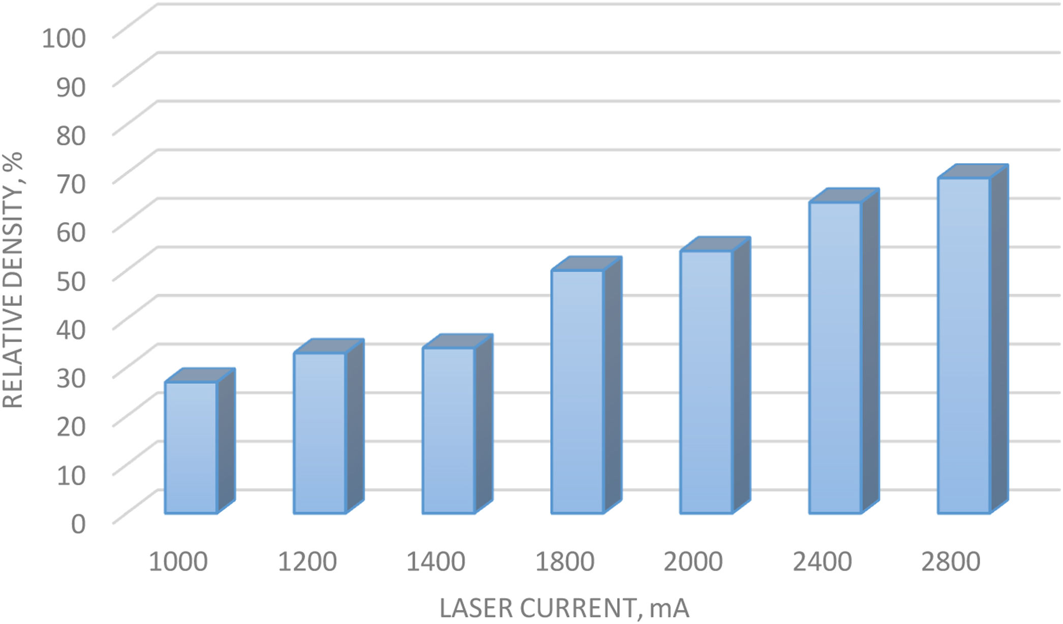
The laser current is considered to be one of the key parameters in AM process. A low current is not sufficient to trigger the sintering process. When the ceramic powder is being heated or cooled too fast, huge stress is generated which leads to cracking and poor mechanical performance. To this end, optimizing the current is imperative and it is a topic for extensive research.
To optimize the sintering process, laser current was fine-tuned and the outcome was monitored. It must be underlined that when the feedstocks contained silicon which has a relatively low melting point (1407°C), it was melted involving the liquid phase in the sintering process. Also, the molten silicon served as a “glue” for bonding the silicon carbide.
In Fig. 3.4 the effect of the laser current on the sintering process is illustrated. As an indicator of the sintering process the relative density is considered: higher relative density means the feed was better sintered. As Fig. 3.4 shows, when the laser current was less than 1000mA the sintering process was not initiated. The sintering process takes place when the laser current exceeded 1000mA. However, the samples were very brittle until the laser current was 2400mA. The printed samples were broken when detached from the baseplate.

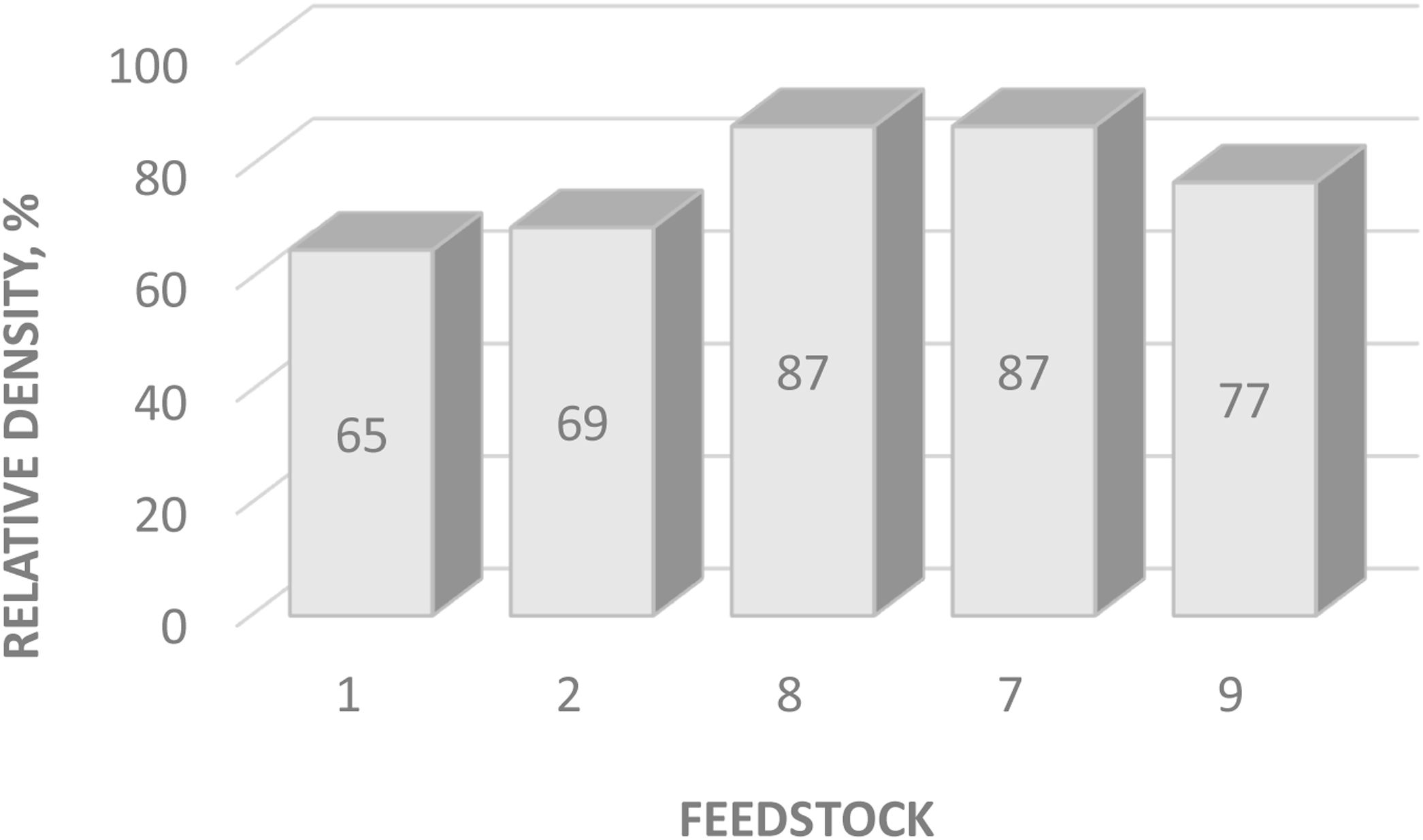
Very similar results were obtained when Feed 1 was changed to Feed 2, i.e., the particle size of the silicon carbide was changed. According to the results (not shown), there were no any significant changes in relative densities when the laser current was 2800mA. Thus, the relative densities were 65% and 69% for Feed 1 and Feed 2, respectively. This finding shows that the narrow distribution of the particle size is not optimal for this feedstock. To be able to improve the sintering process we applied bimodal silicon carbide powder which means powder with different particle sizes were mixed. In the case when bimodal silicon carbide powder was used with a composition of 50wt.% SA37 with 50wt.% F7.6 (Feed 8), the density of the SLS-ed sample reached 87% of the theoretical density.
In conclusion, the narrow distribution of the particle size of silicon carbide regardless of the particle size is not optimal for AM while a mixture of them is.
Effect of additivesThe ultimate goal of this research was also to fabricate ceramic bodies with high electrical resistivity and thermal conductivity. To reach this target we selected two types of as functional additives (i) boron nitride and (ii) yttrium oxide. It is reported that adding boron nitride to raw material significantly improved electrical resistivity [32]. Therefore, we anticipated that a similar effect could be obtained for AM fabricated SiC cases. To explore the effect of the boron nitride we added 10wt.% hexagonal BN into feedstock (Feed 7). The next feedstock was prepared using Y2O3 (Feed 9). Thus, in the 1980s it was estimated that SiC could be sintered to high densities via liquid-phase sintering using Al2O3 and Y2O3 as additives [33]. It was expected that using Y2O3 will change the sintering mechanism and improve the sintering process.
Surprisingly, the phenomenon observed in the classic sintering process, i.e., adding a functional additive to improve sinterability didn’t work in AM. Adding 3% Y2O3 had a reverse effect and relative density was dropped to 77%. Similar results were obtained when the amount of Y2O3 was 5%.
As Fig. 3.5 shows the best results in terms of relative density were obtained for the bimodal SiC feedstock case and BN additive case, here the relative density is estimated to be 87%.

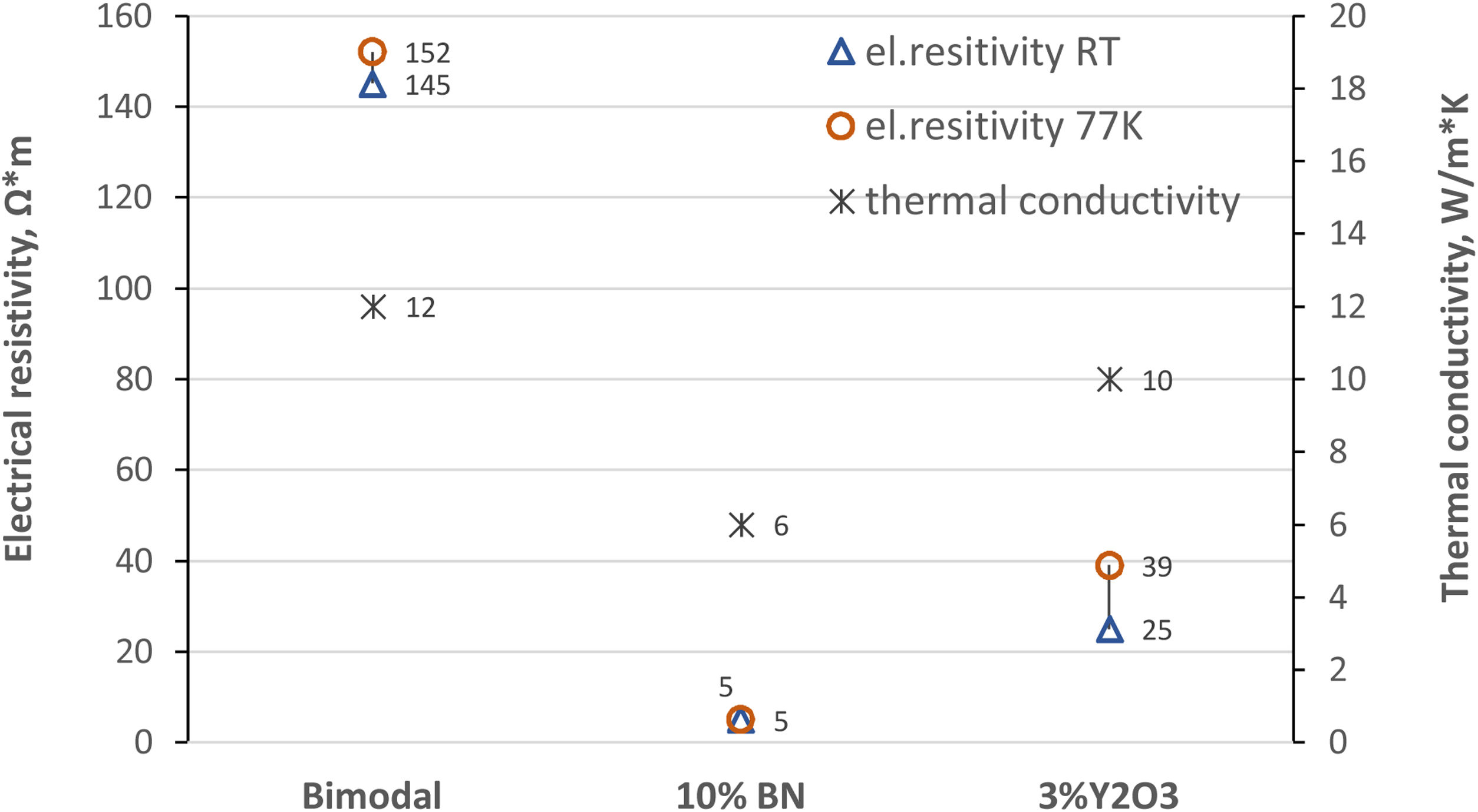
The next quality control parameter of the obtained samples were thermal and electrical properties. According to measured data when boron nitride was used as an additive those properties are sharply decreased (Fig. 3.6).

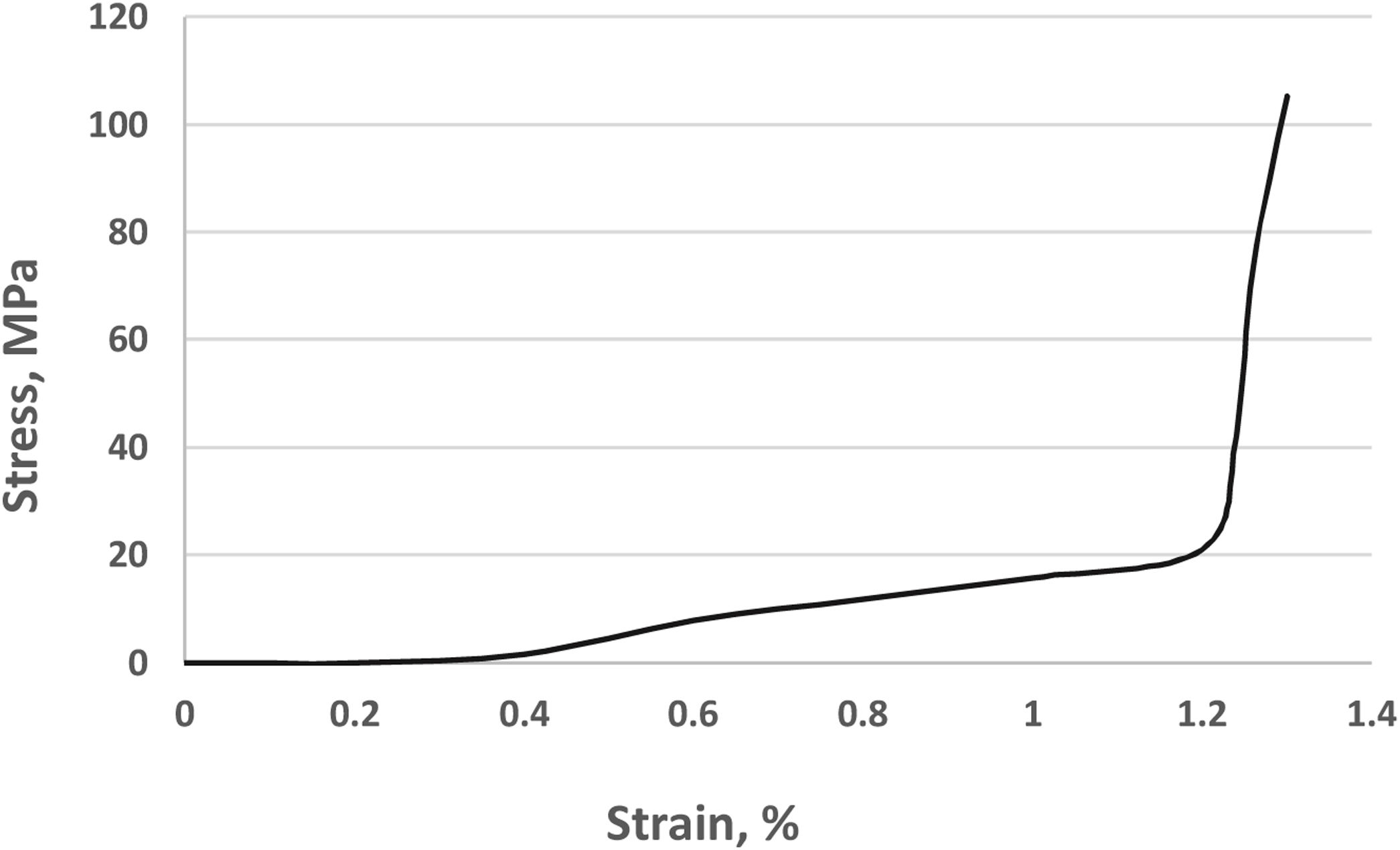
In addition to decreased electrical resistivity and thermal conductivity, BN has also a negative impact on mechanical performance. The mechanical performance of those samples was evaluated by subjecting them to a compress test. The samples were loaded in the universal testing machine and compressed with a 0.05mm/min compressing rate. This low shear rate was estimated to be the best because in this case, it was possible to detect and monitor all changes taking place while the sample was being compressed. The typical SS curve for the compress test is illustrated in Fig. 3.7.

As can be seen, the maximum strain reached up to 1.3%. However sharp changes are observed when the strain exceeded 1.2%. In this range, the curve is linear estimating that elastic deformation took place. When the applied load reached 6.4kN the samples fully collapsed.
The non-linear compression in the first stage when the samples were compressed up to 1.2% was associated with the porosity of the samples. Thus, in this range, the sample was compressed because of residual pores in the mass. When the porosity was physically eliminated the samples started to compress into a fully dense body. At this moment the cure sharply increases and shows leaner characteristics.
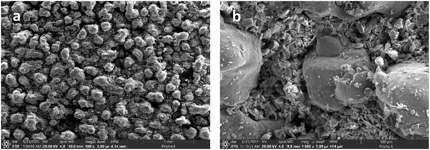
Microstructure analyses confirmed that the sample had a granular structure, and the grains were well visible (Fig. 3.8). The content of the fused part was almost invisible which verifies that the sample was poorly sintered when the current was 2800μA. One can assume that the sample may have a low modulus which was confirmed by the SS curve. It was estimated that Young's modulus for this sample was 27.8±0.2 GPa which is far below the fully dense silicon carbide Modulus (around 420GPa).
 low and (b) high magnification at laser current 2800mA.")
These unexpected results associated with the BN additive could be explained by the formation of 2D BN layer on a silicon carbide particle. Thus, according to Kim et al. [34] when 10% hexagonal born nitride was added to silicon carbide electrical resistivity decreased. This was explained by N substitution for C sites in the 6H–SiC lattice, which acts as donors for supplying carriers to the conduction band.
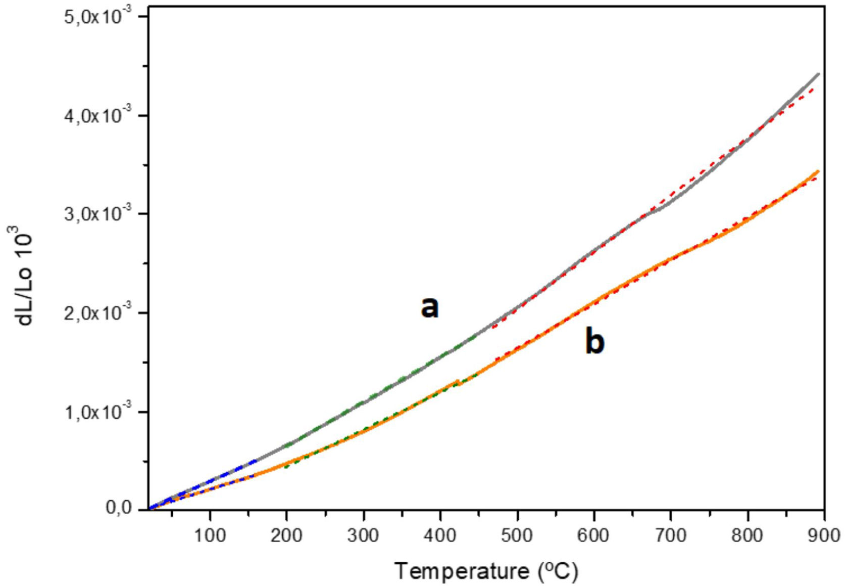
Fig. 3.9 shows a comparison of the samples fabricated from Feed 7 and Feed 8. As can be seen when BN is used the CTE is higher in all temperature ranges (Table 3.1). This is reasonable because the CTE of the pure BN (1–36×10−6K−1 at 20–1000°C) is much higher compared to that of SiC.
 Feed 7 and (b) Feed 8.")
Replacing BN with Y2O3 improved the electrical and thermal properties: however, it was still far below than bimodal Feed case.
Based on these results it was concluded that the best feedstock for AM is the raw material with bimodal SiC components.
Laser current effect on bimodal feedTo optimize laser current, we evaluated the sintering process of Feed 8 with the composition of 20% Si–80%SiC [50% SiC-SA37–50%SiC SiC– F7.6] using 2800mA and 3000mA laser current.
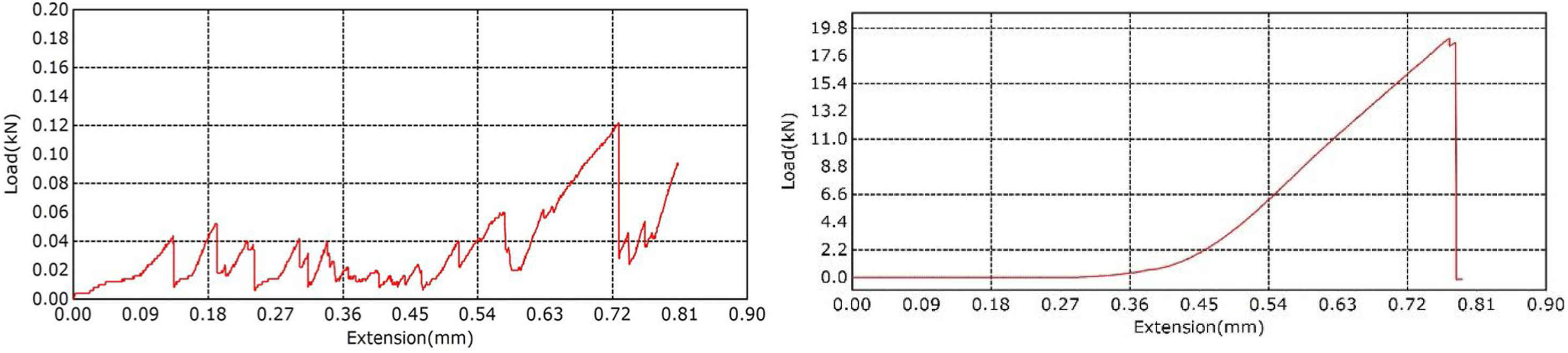
The mechanical performance of those two samples was tested and the results were illustrated in Fig. 3.10.
 2800mA and (b) 3000mA current.")
It was obvious that the two samples had different responses to mechanical loading. The sample fabricated at 2800mA laser current showed a pulsing curve, i.e., the load was increasing then suddenly drops and again escalates. The maximum load was reached when the strain reached to 7% and the load was 0.12kN. This kind of behavior of the cure was caused by the high porosity of the sample. Thus, when the sample was compressed the load increases but the walls of the pores collapse, and the upper layer of the sample was destroyed. Because this layer was collapsed the load was sharply dropped near to 0. Then again, the next layer started to resist against compression, and the applied force increased. At the end entire sample was destroyed.
Fig. 3.11a shows the microstructure of this sample sintered at 2800mA laser current. It can be observed that although there are fused areas still large pores remain. There are well visible particles which means the sintering process was not fully completed. This clearly indicates that the 2800mA laser current is insufficient to print dense samples.
 2800mA, and (b) 3000mA.")
Further, increasing the laser current significantly changed the behavior of the SS curve. As Fig. 3.11b illustrates the load was near zero until 270 um displacement, then it sharply increased linearly until force reached to 18,980kN, and then the sample raptured. This grandiose increased of mechanical strength indicated that the sintering process was completed successfully and a highly dense sample was obtained. The modulus for this sample is estimated to be 59.8±0.3GPa which was significantly higher than previous samples.
Microstructure analyses show that applying 3000mA laser current was sufficient for successful sintering. There is no any remained large pores and the particles are well sintered.
This experiment concluded that the low laser current is not enough to reach the required temperature i.e., around 2100°C. Increasing laser current led to an increase in the sintering temperature and as a result the sintering was more complete, and samples had much better performance. Thus, the electrical resistivity of Feed 8 SLM-ed at 3000mA increased up to 225.34Ωm at cryogen condition (77K) and 217.06Ωm at room temperature. For comparison, the values for samples fabricated at 2000mA laser current was 152Ωm and 145Ωm, respectively.
ConclusionThe effect of feedstock composition, particle size distribution, and laser current were explored to optimize raw material composition and process parameters. It was estimated that feedstocks with a narrow range of distribution of the particle size have poor sinterability. When two different powders with different particle size distributions were combined the sintering process improved significantly.
A functional additive such as BN had a negative effect on electrical resistivity and thermal conductivity properties. Thus, adding up to 10% BN into feedstock the electrical resistivity dropped by about 30 times and thermal conductivity decreased around 2 times. Apart from those properties the mechanical performance of the sample also was low. The Modulus extracted is around 2.7GPa.
Replacing BN with Y2O3 slightly improved electrical resistivity and thermal conductivity; however, it was still far below compared to that of feeds containing bimodal SiC.
It was estimated that the optimal sintering condition was 3000mA laser power and in this case, the modulus increased up to 59.8GPa.
The authors want to thank EIT Raw Materials for the financial support to carry out this part of the work (AGREEMENT NO 19458-BCLC-COVID BOOSTER-2020-8). The authors thank to Enterprise Incubator Foundation for financial support in the frame of Innovation Matching Grants (contract number 08/2021/IMG).