

Yttrium aluminum garnet (YAG) with cerium admixture (Ce:YAG) was plasma sprayed using two different devices – gas-stabilized plasma (GSP) torch and water-stabilized plasma (WSP) torch. Coatings on stainless steel as well as self-standing plates were produced. Besides microstructure and crystallographic characterizations, dielectric tests were performed on these coatings. They included capacitance (i.e. relative permittivity), loss tangent and volume resistivity measurements. After spraying, the YAG crystal phase was preserved without any decomposition, but an amorphous fraction was detected in the as-sprayed coatings deposited by both processes. The dielectric behavior of the coatings was influenced by imperfections like splat boundaries, pores and thin cracks. The Ce:YAG samples were successfully plasma sprayed by both spray techniques. Selected aspects of wear were measured and compared with a single-crystal. The dielectric properties are comparable with the single-crystal and highly promising, particularly the loss tangent with values so low that they were not found in any other as-sprayed ceramic coating.
Se proyectó con plasma granate de itrio-aluminio (YAG) con aditivo de cerio (Ce:YAG) utilizando dos dispositivos diferentes: antorcha de plasma estabilizado con gas (GSP) y antorcha de plasma estabilizado con agua (WSP). Se produjeron recubrimientos sobre acero inoxidable y placas autoportantes. Además de las caracterizaciones microestructura y cristalográficas, se realizaron pruebas dieléctricas en los revestimientos. Incluyeron medidas de capacitancia (es decir, permitividad relativa), factor de pérdida y resistividad de volumen. Después de la proyección, la fase cristalina de YAG se conservó sin descomposición alguna, pero se detectó una fracción amorfa por ambos procesos. El comportamiento dieléctrico de los revestimientos fue influenciado por imperfecciones como límites, poros y grietas delgadas. Las muestras de Ce:YAG de proyección con plasma con éxito mediante ambas técnicas sin una pérdida irreversible de la fase cristalina deseada. Las propiedades dieléctricas son prometedoras, particularmente el factor de pérdida con valores tan bajos que no se encuentran en ningún revestimiento cerámico pulverizado.
The yttrium aluminum garnet (YAG) with chemical formula Y3Al5O12 is a material broadly used in form of single crystal as well as ceramics [1–4]. The compound 3Y2O3·5Al2O3, commonly called yttrium aluminum garnet (Y3Al5O12, YAG), adopts the cubic garnet crystal structure. Nevertheless, electrical properties of polycrystalline Ce:YAG were not studied enough up to now.
Ce:YAG single crystal is characterized by excellent mechanical properties and it is industrially produced as a chemically resistant scintillator. Mechanical properties enable production of Ce:YAG scintillation screens down to a thickness of 100μm, Ce:YAG detectors are excellent for electron microscopy, beta and X-ray counting, electron and X-ray imaging screens. The popularity of this material consists in its relatively fast decay, high light yield, and low production costs. However, the Ce:YAG single crystals usually contain various unwanted structural defects which can result in non-radiative recombination and in delayed luminescence decay (afterglow).
In polycrystalline ceramics severe scattering of light takes place at defect sites such as pores and grain boundaries [5]. In order to achieve good dielectric properties, it is important to reduce the presence of pores and secondary phases. YAG is a stoichiometric compound and any shift from the stoichiometric composition would produce secondary phases [6]. Low amount of Ce dopant is not detectable by X-ray diffraction [7]. Compared to single crystal and fine-grained sintered bulk, plasma sprayed coatings should have high level of internal stress.
Plasma spray process is used to fabricate coatings thicker than 50μm from a wide range of industrial materials, including ceramics. The principle of thermal spray is following: (i) melting of a material feedstock powder, (ii) accelerating the melt and (iii) impact on a substrate where rapid solidification and deposit build-up takes place. The melting temperature is achieved in an electric arc, which ionizes the plasma forming medium – either gas or water. In case of the used WSP system water is the medium. The plasma jet accelerates the externally fed-in molten particles to the target substrate, where the material solidifies forming a deposit. The deposit is built-up by successive impingement of the individual flattened particles called “splats”. Successive passes of the plasma jet over the substrate (i.e. spray trajectory) are carried out by a robotic arm or similar programmable manipulator.
Feedstock powder is introduced into the water-stabilized plasma jet outside the gun using one or several injectors. These injectors can be positioned at various angles and distances from the exit nozzle for different feedstock chemistry and sizes. Temperatures in this jet are high: the maximum can reach 30000K, compared to about 15000K maximum for GSP. Even when the velocity of plasma jet is between 5000 and 7000ms−l at the nozzle, compared to 1000–1500ms−l for GSP, the impact velocities of deposited particles are about the same or slightly lower than for GSP spraying. This is caused by a lower acceleration of injected particles due to the lower density of plasma. WSP uses for stabilization of plasma normal tape water and by this way is it less expensive than GSP utilizing argon gas. The ability to coat larger area within the same time unit is one typical advantage of WSP over GSP.
References to YAG plasma spraying are relatively rare and only consider its pure form [8–11]. A metastable hexagonal yttrium aluminate (H-YAlO3) was the major phase, when YAG was plasma sprayed. The crystallinity of the as-sprayed YAG coatings was the highest at high power and short stand-off distance used [8]. In the same paper the thermal post-treatment (annealing) was mentioned as an efficient way to get highly or fully crystalline coatings with the desirable YAG phase. We accomplished similar experience in own previous study [7].
Sintered YAG ceramics is a superior microwave dielectric material, despite the fact that its quality factor Q is approximately a half, compared to that of the single-crystal [12]. This means the loss tangent Tanδ about 0.0001 for the polycrystalline material. The exact values depend mainly on the production technology. Sintering for 24h at 1650°C would prevent the formation of secondary phases [12] and led to lower Tanδ compared to YAG containing approximately 1% of TiO2[13]. Relative permittivity is reported within values between 9.9 and 10.6 [14–16]. The electric resistivity of Ce-doped YAG is lower than that of the pure YAG at room temperature [17].
The aim of our work was to test the influence of the plasma spray process on the structure and dielectric properties of Ce:YAG material. According our knowledge, Ce-doped YAG was never electrically characterized in the form of a plasma sprayed coating. Cerium doping is important in optoelectronics and we could expect a change in the activation energy compared to pure YAG. By this way it would modify the dielectric behavior as well. This aspect of the doping is not thoroughly addressed in the existing literature. We used Ce:YAG single crystals crushed and sieved to form a spray feedstock powder. We preferred this approach against the use of precursors with different composition (i.e. in situ plasmachemical synthesis) which is a more frequently reported approach even for undoped YAG [8,10]. The Ce:YAG was deposited with the water-stabilized plasma (WSP) [18] and gas-stabilized plasma (GSP) spray techniques. All coatings were sprayed at normal atmospheric conditions in order to compare these two processes. The main motivation of our research was to produce large-area low-loss dielectric thick films by plasma spraying. The microstructure and dielectric properties are discussed in comparison with Ce:YAG single-crystal that represents a defect-free bulk material.
ExperimentalPowders and sprayingSingle crystals of YAG doped with 5mol.% of Ce were received from the producer (Crytur, Czech Republic). Fragments with the same physical nature but with shapes and sizes different from real industrial single-crystalline products were milled end sieved into powder for spraying. Two different powder size classes (i.e. different optimum powder size for WSP: 63–100μm, and GSP: 20–63μm) [7] were prepared.
Spray setting details were listed in our earlier work [7]. Let us here summarize the main parameters: torch power was 100kW for WSP and 34kW for GSP; stand-off distance 250mm for WSP and 150mm for GSP; powder feed-rate 15kg/h for WSP and 3kg/h for GSP; powder carried by air at WSP and by argon at GSP.
Similar spray trajectory brings higher substrate temperature rise with WSP compared to GSP, because of higher power of the WSP spray torch. Since the WSP process applies substantially higher thermal load onto the sprayed material, the risk of overheating and coating damage was high. Therefore, only rather thin coatings were realized by WSP (i.e. a short spray run). Such coatings could not be separated from the substrate and handled as free standing.
Coating characterizationDensity was examined by the helium pycnometry (AccuPyc 1330 V3.03, Micromeritics, USA). The porosity of the coatings was analyzed on cross section optical images processed using an image analysis (IA) software. Five images of coatings with 400-times magnification of the cross section were analyzed per sample. For a more precise description of the porosity, additional criteria were introduced [19]. Surfaces of the coating were observed by Scanning electron microscope (Tescan VEGA3) running in secondary electron (SE) mode and applying beam voltage 30kV.
The phase compositions were analyzed with X-ray powder diffractometer D8 Discover (Bruker, Germany) with the Bragg-Brentano focusing geometry, equipped with 1D LynxEye detector and xyz positioning system based on laser. Filtered Cu Kα radiation was used in the angular range from 10° to 90° 2theta.
Electrical measurements were performed on coatings as-deposited with the metallic substrate in the case of WSP, but on free-standing coatings in the case of GSP. The surface of specimens was machine polished in order to eliminate surface roughness. Aluminum thin film electrodes were sputtered under reduced pressure on the frontal side of each sample. A three-electrode measurement fixture 16451B (Agilent, USA) was used to apply the electric field and read the dielectric parameters. In case of the WSP coatings the substrate played the role of a backside electrode, whereas for the GSP samples the back side was covered by sputtered aluminum too. The electric field applied was perpendicular to the substrate surface. Capacitance was measured in a frequency range from 160Hz to 100kHz (i.e. radio-frequency band, RF) using a programmable impedance analyzer LCR Hi-Tester 3522-50 (Hioki, Japan) with the applied voltage 1V (±0.02V) AC. Relative permittivity ɛr was calculated from measured capacitance (CP) and specimen dimensions since ɛr is directly proportional to CP according to Eq. (1).
where εr is the relative permittivity of the sample, ɛ0=8.854×10⁻¹²Fm−1 is the vacuum permittivity, k [m] is thickness of the sample [20] and S [m2] the electrode area. The same setup was used for the loss tangent Tanδ measurement at the same frequencies as for the capacitance.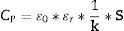
Electric DC resistance was measured with a special resistivity adapter – Keithley, model 6105 (Keithley Instruments, USA). The electric field was applied from a regulated high-voltage source and the values collected via a multi-purpose electrometer 617C (Keithley Instruments, USA). The voltage value was set as 100±0.05V DC and the exposure time as 10min. Volume resistivity was calculated from the measured resistance and specimen dimensions according to Eq. (2).
where R is the resistance of the sample [Ω], S the sample area [m2] and L the sample thickness [m].
Temperature dependencies of relative permittivity and loss tangent were measured for selected samples between 25 and 400°C. Switchboard model 7490A (Agilent, USA) and thermometric chamber model 3140 Isocal Venus (Isotech, UK) were applied.
The surface roughness was recorded by the Surtronic 3P (Taylor Hobson, UK) using contact technique. Five tracks with 25mm path were recorded for each sample and averages of the Ra parameter calculated.
Wear resistance was tested as an important characteristic of mechanical quality of the coatings. Slurry abrasion response (SAR) of coatings was measured according to a modified procedure based on ASTM Designation: G 75 – 95 [21]. SAR test is based on measuring the mass loss rate of a standard-shaped block (7.5mm×12mm×25mm; the self-standing ceramics glued on a plastic holder) when lapped in a slurry. The test consisted of four increments with mass loss being measured at the end of each increment. The applied force was 22N per specimen. After each run the specimens were ultrasonically cleaned and weighted. The slurry consisted of 150g of water and 150g of alumina powder with sizes from 40 to 50μm. Accuracy of the measurement is approx. ±5%. The wear resistance is expressed as Inverse wear rate (IWR), representing the distance passed by the samples in the slurry until one cubic millimeter of the material is worn-out. The higher the IWR, the better the wear resistance.
Since the coating samples were completely consumed (i.e. worn out) by the SAR test and therefore subsequent observation of worn surfaces was not possible, we decided to add also a scratch test. The scratch testing was performed according to ASTM 149C-1624 standard [22] using Revetest RST device 150 (Anton Paar, Austria). According to the standard, thickness of hard (oxide) coatings should not exceed 30μm. The original coatings thickness was therefore reduced by grinding whereas and the final surface smoothened by #1200 sand paper grinding. A linearly increasing load (0–100N) was applied on the crystal sample, GSP coating and WSP coating, respectively, and the critical force was determined [23].
A confocal (408nm laser based) microscope VK-X1000 (Keyence, Japan) was used for the observation of scratches and reconstruction of three-dimensional images.
Results and discussionPhase analysisOnly one crystalline phase, the YAG phase, i.e. Y3Al5O12 (PDF No. 033-0040), Fig. 1, was detected by XRD in the coatings. The YAG composition at phase equilibrium represents 37.5mol.% of Y2O3 in Al2O3[24,25]. However, a pronounced extension of the existence of stoichiometric YAG toward the Y2O3-rich side of the phase diagram was reported [9]. A high proportion of the material of both coatings was in the amorphous form (the halo at low angles 2θ degrees), Table 1. The reason for such amorphization, many times observed in the past [26,27], is the rapid cooling of the coating during plasma spraying. Cerium-containing phase was not detected, which suggests that Ce3+ ions were, to some extent, dispersed preferably in the amorphous matrix rather than completely incorporated into crystal lattice [28]. Crystallinity of the WSP coating was higher because of smaller thermal gradient between the material melting point (1940°C) and the quenching temperature at WSP process (c.f. 240°C maximum inter-pass surface temperature detected at WSP, compared to 130°C at GSP).

Results of Rietveld refinement – lattice parameter a [Å] and mean size of coherently scattering domains D [nm] (i.e. crystallite size). Crystallinity estimated from diffraction in the region from 22° to 68° 2theta.
| Sample | a [Å] | D [nm] | Crystallinity [wt.%] |
|---|---|---|---|
| GSP | 12.0167(7) | 78.1(19) | 7.27 |
| WSP | 12.0123(5) | 106(2) | 35.96 |
| Single crystal | n.a. | n.a. | 100 |
The occurrence of Y3Al5O12 only, both in GSP and WSP coatings, is a significant distinction from coatings sprayed from precursors [25] which did not reach the desired phase composition of single-phase cubic YAG. Cerium did not create any individual phase and is not detected by XRD; however, it could be present as substitutional or interstitial atom in a fairly complex cubic lattice with Ia−3d space group. The presence of Ce3+ in YAG garnet structure [29] is indicated by the increase of lattice parameter compared with pure YAG, which is 12Å [29]. The increase of both the unit cell parameters, Table 1, and bond lengths indicate some alteration, implying that Y3+ atoms (180pm) were partially substituted by larger Ce3+ (185pm) in our samples.
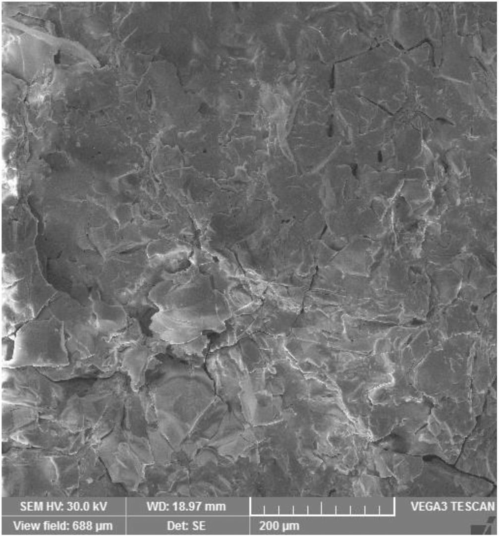
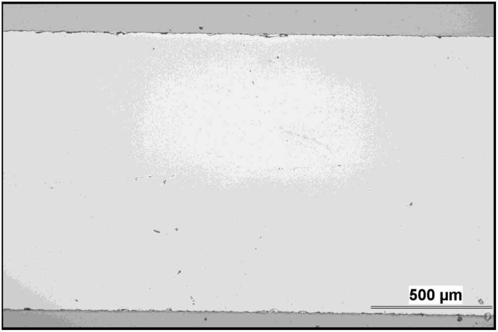
Microstructure and wearMicrostructure of the coatings is presented on micrographs of surfaces taken by SEM-SE, Figs. 2 and 3. The GSP coating was self-standing with thickness comparable to the available single-crystal sample (1180±5μm, c.f. Fig. 4), whereas the WSP coating was relatively thinner (500±15μm). Surface of GSP exhibits predominantly well flattened lamellas whereas the surface of WSP coating is more cracked and faceted, c.f. Figs. 2 and 3. The cracking of WSP could be due to thermal mismatch (at low thickness) with the substrate, but could also reflect higher quantity of unmelted and improperly melted particles of the feedstock powder. This issue brings the question whether the ratio of crystalline phase in the coatings is just a consequence of such unmelted particles.

GSP coating, surface, SEM-SE, same scale like Fig. 3.


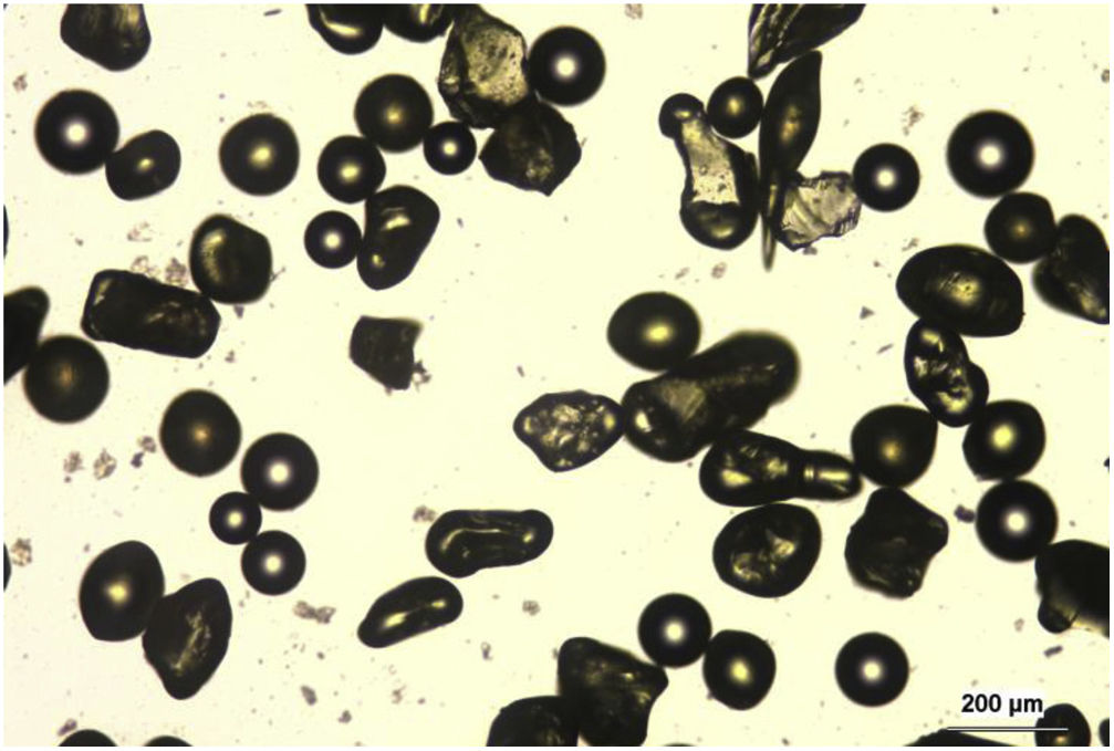
The WSP spray experiment was accompanied by collecting the as-solidified particles, after leaving the plasma jet, into a liquid, instead of a substrate. These so called free-flight particles (FFP), Fig. 5, were quantified. Two types are easily distinguished and were counted manually using 10 different images. The total 412 particles included 64% of perfectly rounded particles (i.e. molten in plasma and solidified) while the rest 36% were irregular. Based on this observation we must admit that the crystalline proportion in the coatings is, at least partly, inherited from the feedstock powder via incomplete melting of significant proportion of particles.

Porosity of the plasma coatings is of course non-zero. The measured area fraction of pores was over 3%, c.f. Table 2. Circularity (CIR) describes pore shapes. Zero (0) value holds for crack-like pores (possible anisotropy not considered), while unit (1) value represents ideally globular pores. Minimal detected circularity CIRmin is similar for both coating types – cracks or flat pores were present in both coating types. The single-crystal had different character; its pores were remarkably finer (E.D. under 1μm), porosity area fraction reliably under 1% and circularity of pores rather high, over 0.9. All these values are summarized in Table 2. However, the pore size (“equivalent diameter”, E.D.) was nearly twice as large for the WSP coating. Number of pores per mm2 was correspondingly higher for GSP, which means that this coating had high amount of rather fine pores while against the WSP coating led to smaller quantity of larger pores. Considering the differences between spraying and the single-crystal production route, the observed differences between the crystal and coatings lie within frames of expectations. Concerning the differences between GSP and WSP, the finer feedstock powder and higher thermal gradient associated with GSP led to finer pores.
Image analysis of pores, wear resistance results (IWR), critical force at scratch test Lc and electrical resistivity (at room temperature).
| Sample | Porosity [%] | Pore size – E.D. [μm] | Pores per mm2 | CIR | CIRmin | IWR [mmm−3] | Lc [N] | Resistivity [Ωm] |
|---|---|---|---|---|---|---|---|---|
| GSP | 3.6±0.3 | 5.90±1.00 | 725±61 | 0.46±0.04 | 0.058 | n.a. | 48 | 1.58×10¹² |
| WSP | 3.2±0.4 | 10.88±2.95 | 273±86 | 0.35±0.04 | 0.056 | 153 | 45 | 3.24×10¹³ |
| Single crystal | 0.4* | 0.78* | n.a. | 0.92* | 0.069* | 418 | 80 | over 1014 |
* NOTE: not fully comparable because of different magnification and image resolution.
Correspondingly, the surface roughness of GSP was lower – the Ra parameter showed values of 25.4μm, 9.5μm and 0.6μm for WSP, GSP and crystal, respectively. The density of the GSP as-sprayed coating, determined by He-pycnometry, was 4.1665g/cm3, whereas the theoretical density of YAG is about 4.56g/cm3. This is 91.4% of the theoretical density for GSP, whereas its porosity is only 3.6%; also, some 5% of the density drop should be caused by less dense amorphous material.
Wear resistance of the coating (WSP) was substantially lower compared to the single crystal, Table 2. Such a difference is expectable considering the extremely low porosity of the crystal and also its high microhardness, over 20GPa [7]. WSP coating, being harder than GSP [7], is supposed to exhibit higher wear resistance, however, we did not have a suitable GSP sample for this test. When we are comparing the wear resistance of the WSP coating with similar ceramics, we have IWR values between 120mmm−3 and 210mmm−3 for Al2O3, depending on various processing conditions [30]. On the whole we can consider the IWR parameter of the Ce:YAG coating to be typical for hard ceramic coating materials.
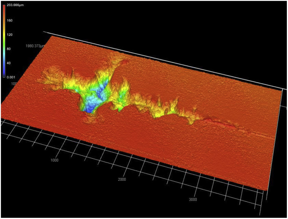
The average critical force Lc measured by scratch test reached 45–50N (Table 2) for both coatings. Such values are significantly lower than those for the single crystal, i.e. 80N. In relevant literature sources we can find a wide dispersion of values for plasma sprayed ceramics, e.g., 60N [31] or 80N [23] for ZrO2, 35N for SrZrO3[32], 42N for crushed powder based Al2O3[33], 62N for nanostructured Al2O3[33]. Note that the measured critical force did not actually correspond to the full detachment of the YAG:Ce layer from the substrate – such a condition was never reached in the experiment. However, additional observation of the worn surface was performable only for the crystal, whereas the coatings were broken by the maximum applied load (i.e. crack in both the coating and substrate – alumina coupons in this case). A path of the scratch on YAG:Ce crystal is visible in Fig. 6. Some groves with maximal depth over 160μm, oriented perpendicularly to the scratching direction, were found.
Dielectric properties
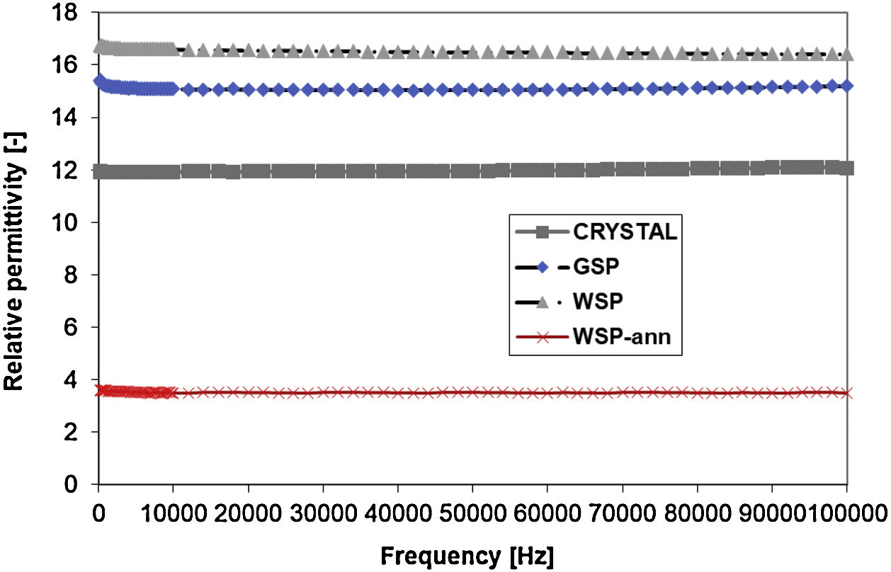
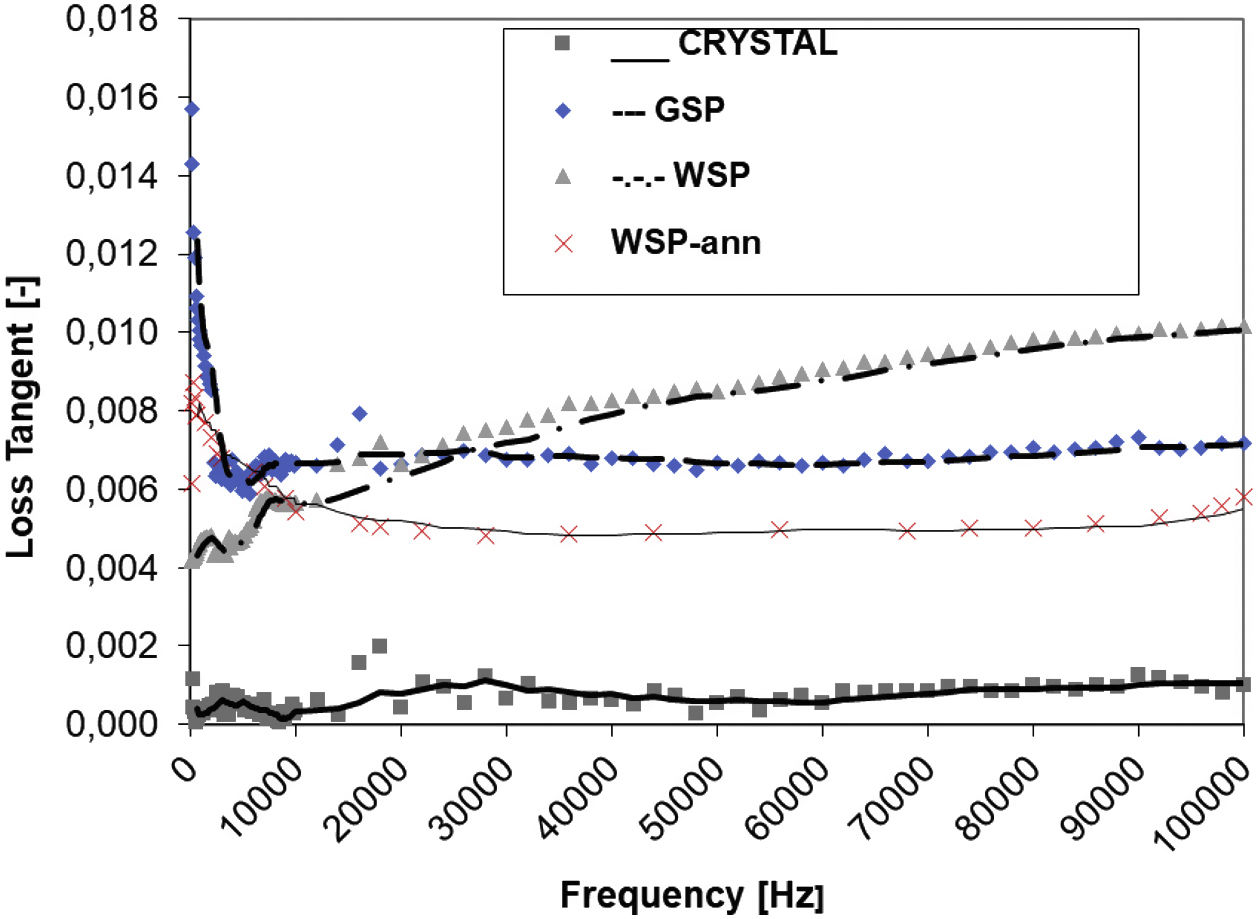
The dielectric response to AC field is displayed in Figs. 7 and 8. Relative permittivity, Fig. 7, of the WSP coating is higher, about 17, whereas GSP samples have the average value about 15 and the single crystal 12 exactly. Both coatings have very stable course of permittivity versus changed frequency. The loss tangent Tanδ reaches remarkably low values, seldom accessible for any other studied ceramic plasma sprayed coating. Loss tangent, Fig. 8, of the GSP coating is higher (with values of 0.012–0.007) at low frequencies below 30kHz. At higher frequencies the rather stable value of about 0.007 is preserved. The WSP coating's loss tangent starts from 0.004 at low frequencies and meets the value 0.009 (higher than GSP coating) at the maximum measured frequency 100kHz.


The phase composition of the coatings could be responsible for the observed differences – the WSP coating has higher crystallinity and slightly higher resistivity, Table 2. The resistivity of both coatings is several orders of magnitude higher than the value of Ce:YAG prepared by sol–gel technique (with resistivity about 108Ωm [17]). Compared to our single crystal sample (with the resistivity outside the range measurable by the available equipment), values of both coatings are slightly lower.
Polarization of defects, admixed cerium ions and crystallite boundaries contribute to the entire polarization, responsible for the permittivity of both coatings. The loss tangent of the single crystal is particularly low due to the absence of any coarse defects. The loss tangent of coatings is higher, because of microstructure features responsible for polarization [27]. This is namely porosity resulting from shadowing effect during the splashing of particles on previously arrived splats, voids or gas inclusions between splats, unmelted particles, and also from explosion of overheated particles on impact [8]. WSP has lower loss at low frequency because of lower porosity but higher loss at higher frequency most probably because of larger crystallite and pore size, c.f. Tables 1 and 2. The resistivity of WSP coating is also higher, most probably because of higher crystallinity. Cerium ions are also more suitable for contributing to the charge transfer in the amorphous environment than in the crystalline one. More amorphous Ce:YAG should be therefore less resistive, which is the case of GSP. Finally, the WSP coating could be considered a slightly better RF dielectric than the GSP coating.
Electrical conduction in solids is generally determined by two parameters: carrier concentration and carrier mobility [34]. Oxides are predominantly ionic compounds. In general, the overall transport properties of oxides are determined by defects caused by both – impurities and deviations from stoichiometry [34]. The observed increased resistivity of coatings compared to bulk polycrystalline Ce:YAG values might result from the trapping of charge carriers (both electrons and holes) at the grain boundaries and fine cracks. Interesting fact is that the predominantly amorphous character of both types of coatings was not associated with strong and detrimental differences compared to single crystal.
The periodicity present in crystals allows us to describe electrons as Bloch waves. The electrical resistivity is then due to the scattering of electrons from crystalline imperfections, such as impurities, vacancies, dislocations, or from other electrons or phonons. However, in order to interpret the electric transport in amorphous materials we should consider the dependence on the localized character of conduction electrons, as well as on the strength of the electron-phonon scattering [35].
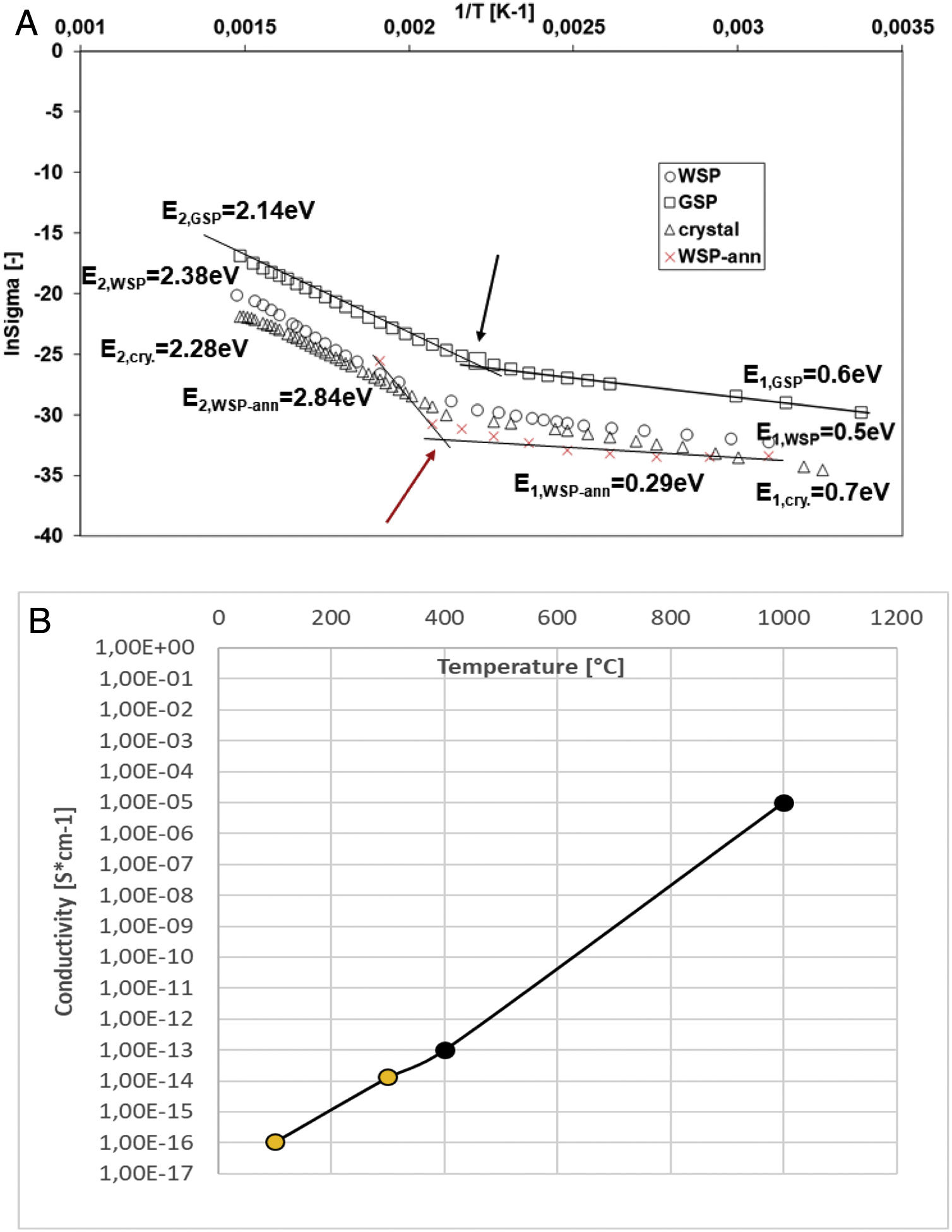
Fig. 9a shows a plot of lnσm (σm is conductivity [Sm−1]; reciprocal value to resistivity) versus 1/T (T is temperature [K]), where the dots are the experimental data for the temperature interval from room temperature to 400°C, measured at 500V DC. The activation energy values were calculated from the least-squares fit to the points. The activation energies (E) of the samples were calculated using the Arrhenius relation σ=σo exp(−Ea/KBT), where KB is the Boltzmann constant and T is temperature [K].
![(a) Activation energy based on DC conductivity measurement. (b) Change of conductivity with temperature, our single-crystal sample (light points) and data from literature [38] (dark points).](https://static.elsevier.es/multimedia/03663175/0000006100000005/v1_202211050707/S0366317521000145/v1_202211050707/en/main.assets/gr9.jpeg?xkr=ue/ImdikoIMrsJoerZ+w997EogCnBdOOD93cPFbanNd3TCEZuNxhudow/+3Hrh9WJc+mtnYSSPL9K6mfMWVj1nfXA6SvATi2HsXEvLFmX4TQScWI4lywpGTkPusm/D3b8+LJ9VKqxGpm9sSlV1rZ//pHZ5M0U9w3ewGe85zRxp33xGwkUOeKyr3RkcPHLAYAPnRrPzNch/ezXQ8dB/O3mM+2tJ28SYSXT6TqJc84ovXXksoWptLaeLQqwT2crJNQn3+jDXKUUDaQhCK55+wJKsiSl4w6CDd6FPRxY56IBPBJ1zqF8kTTUbuvpRRjv6fE "(a) Activation energy based on DC conductivity measurement. (b) Change of conductivity with temperature, our single-crystal sample (light points) and data from literature [38] (dark points).")
(a) Activation energy based on DC conductivity measurement. (b) Change of conductivity with temperature, our single-crystal sample (light points) and data from literature [38] (dark points).
The slope of the plots in the considered temperature range has changed, indicating that a change in the conduction mechanism took place [35]. Conductivity of all three samples at higher temperature (corresponding to E2) is higher, which is common behavior of most dielectric ceramic materials [36,37]. The activation energy values calculated from Arrhenius relation are E2=2.14eV for the GSP coating, E2=2.28eV for the single crystal, and E2=2.38eV for the WSP coating. The value E2 for the single crystal is not far from reported value 2.32eV [38] obtained at pure YAG crystal, c.f. also Fig. 9b.
In the lower temperature region (approx. under 200°C), there is a smaller slope of the linear variation in conductivity dependence approximation with temperature. The activation energy values calculated from Arrhenius relation are E1=0.5eV for the WSP coating, E1=0.6eV for the GSP coating, and E1=0.7eV for the single crystal. The activation energy of Ce-doped YAG was found to increase with increasing temperature. Such a relationship between conductivity and temperature [38] suggests that a transition from dominating dopant mechanism at lower temperatures to intrinsic mechanism at higher temperatures occurred [35].
Porosity of GSP coating is slightly higher than of WSP coating and also its activation energy in the low temperature region is slightly higher. According to our opinion, this corresponds with the gas entrapped into pores during the spray process and ionized by the voltage applied during the test. The activation energy E2 of single crystal corresponds to the wavelength 543nm, which is exactly the same value as the maximum of the luminescent intensity of Ce3+:YAG material [29].
To observe the influence of annealing of the plasma sprayed coating on the activation energy and Arrhenius plot, the WSP coating was heat-treated in a laboratory furnace in air for 1h at 1000°C (sample label WSP-ann). Its dependence of conductivity on 1/T is plotted in Fig. 9a by red color. Its activation energy E2 is higher, i.e. 2.84eV, whereas its E1 is lower in comparison with the as-sprayed samples, i.e. 0.29eV. The transition point from E2 trend to E1 trend seem to shift a bit up, to 210°C, c.f. the red (bottom) arrow. However, we were able to test this, slightly deformed, sample only up to 250°C, so the estimation of E2 is less accurate compared to the as-sprayed samples. The transition from dominating dopant mechanism at lower temperatures to intrinsic mechanism at higher temperatures [35] is more pronounced after annealing. This corresponds to the crystallization of the YAG:Ce. The evidence of crystallization during annealing with 1000°C temperature plateau is based on our earlier investigation [7].
Relative permittivity of the annealed WSP coating is markedly lower than for all other samples (red line in Fig. 7). Actually, we have no clear explanation for this behavior since it is even lower than those mentioned in the literature for pure YAG [14–16]. It holds for ceramic materials, that when moisture or impurities like free alkali ions in the structure are present, the “artificial” shift of the permittivity always tends to go upwards. And moreover, the loss tangent is strongly changed at the same time, which is not the case of this particular set of samples.
The frequency dependence of loss tangent Tanδ for this annealed WSP sample is shown by red color in Fig. 8. Compared to the as-sprayed WSP, the frequency dependence drops and stabilizes (versus the frequency change) at value around 0.005. Usually, annihilation of some defects, reached by annealing, diminishes the loss factor of plasma sprayed dielectric ceramics [36]; so, this effect could be found also here.
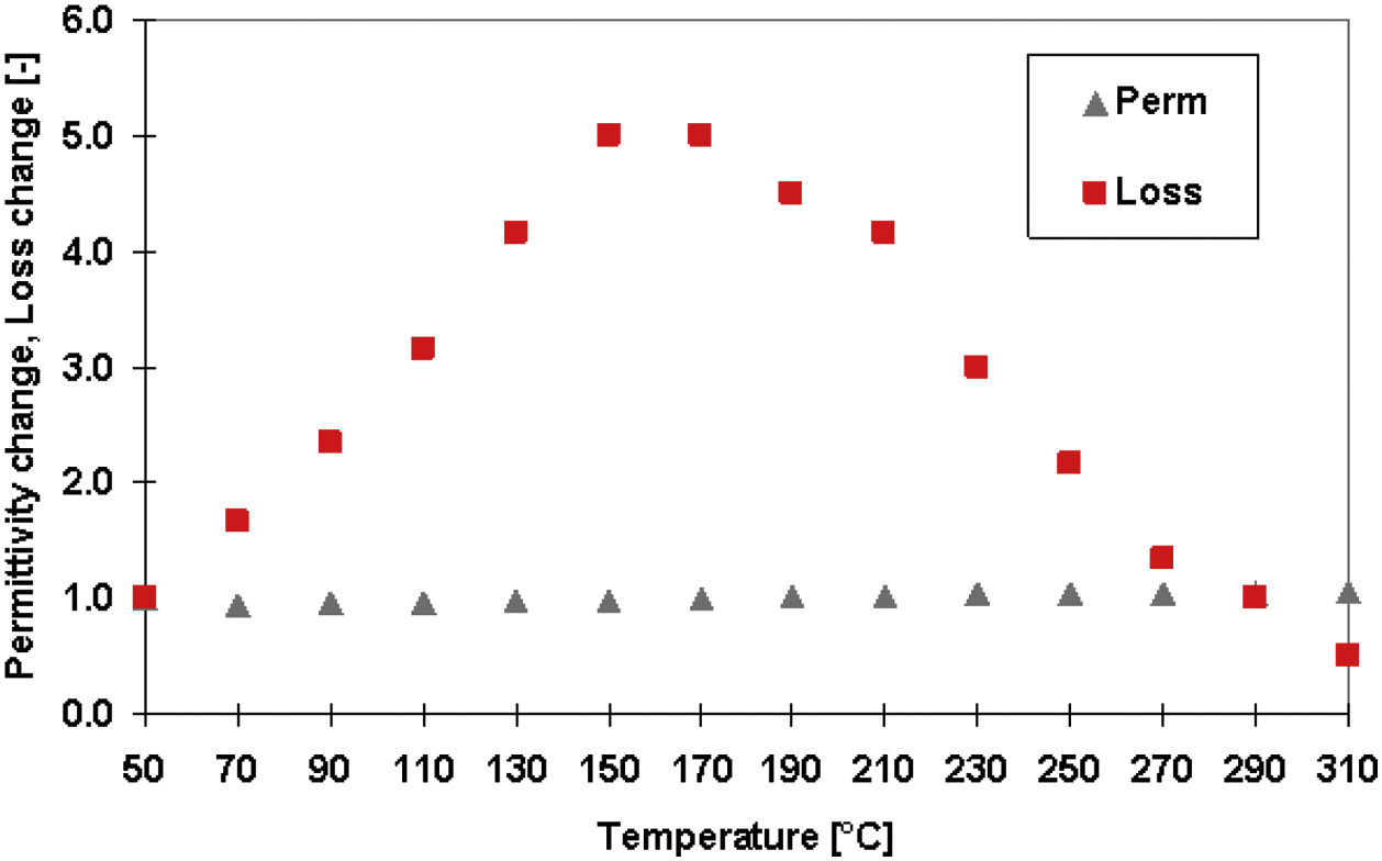
Fig. 10 shows temperature dependence of the relative permittivity and loss tangent for the GSP sample at 1MHz frequency. The values at the low temperature (50°C) were given to be equal to 1, so only the dimensionless change is displayed on the Y axis. We see a stable course of the permittivity across the whole temperature range but the broad peak maximum of the loss tangent centered at about 170°C. This is exactly the temperature, indicated by an (black; top) arrow in Fig. 9a, where the slope of the Arrhenius plot is changed. Conduction mechanism is changed at this temperature and the loss tangent is therefore the highest here. Polarization mechanisms (i.e. those active at 1MHz) are not changed at those temperatures and that is why the permittivity course is without any change.

The fact that the permittivity is constant versus frequency indicates that there are no macro-scale factors (pores, grain boundaries) having detrimental impact on the permittivity. Loss tangent measurement supports this conclusion – i.e. at higher frequencies the WSP coating has the highest loss tangent that is associated with atomic-scale defects. On the other hand, GSP has its maximum loss at low frequencies, which is associated with macro-scale defects. With GSP, more oxygen vacancies should be created in case of Ce:YAG; c.f. the expansion of the crystal lattice, Table 1, which is larger [37,38]. GSP, on the other hand, is more amorphous and the dipoles originated due to an oxygen deficiency in the amorphous structure cannot serve as stable charge carriers in AC electric field.
Suspension plasma spraying is one of the alternatives when a completely crystalline coating is desired. However, the results of phase composition (available for non-doped YAG) are also contradictory. Sometimes the desirable YAG phase was obtained with only trace amounts of YAM (i.e. YAlO3) phase [39], but in another case the YAG phase represented only some two thirds of the coating's mass, the rest being YAM, YAP and other phases with different stoichiometry than YAG [40]. Deeper analysis of the relations between plasma processing parameters and phase composition will be challenging topic for the future research.
ConclusionsYttrium aluminum garnet (YAG) doped with Ce was plasma sprayed using two different processes – gas-stabilized plasma (GSP) and water-stabilized plasma (WSP). Mainly free-standing plates were obtained with GSP whereas WSP was used for thinner coatings adhering on substrates. High amorphous fraction was detected in both types of coating whereas the only crystalline component was Y3Al5O12. Relative permittivity of the coatings was stable during frequency sweep from 160Hz to 100kHz and reached values between 15 and 17, the later for the WSP coating. The loss tangent reached values so low (from 0.004 to 0.009) that they are hardly reachable with any other ceramic plasma sprayed coating. The WSP provided a coating with slightly better radio-frequency dielectric performance compared to the GSP, particularly in terms of resistivity. The measured activation energy of Ce3+:YAG single crystal corresponded to the cited literature, whereas the activation energies of both coating types have similar trends as the single-crystal. The extraordinary insulating character of Ce:YAG, ascertained for the single-crystal sample and given by a combination of high resistivity with low permittivity and low losses, was preserved also with the plasma spray processing. In the case of material produced by a rapid heating/cooling cycle, as thermal spray is, this combination of results has remarkable value for prospective applications.
The authors acknowledge that the GSP spraying was done by S.A.M. Holding, Miletín, CZ. X-ray diffraction measurement and data processing were performed by Z. Pala and M. Dudr, former employees of the IPP ASCR. Scratch test was performed by J. Čížek (IPP) and photography of the wear track by P. Veselý (FEE).