


The work presents a simple solvothermal method for CZTS nanoparticles preparation using hexadecylamine (HDA) as a capping agent. The as-prepared CZTS powder was deposited as ink using Doctor Blade technique onto ceramic tile, as a substrate substituting the typical soda-lime glass. The as-prepared film was thermal treated at different temperatures in order to enhance the thin film crystallinity. CZTS crystal growth onto ceramic tile was obtained successfully for the first time.
En el trabajo se presenta un método solvotermal para la obtención de nanopartículas de CZTS usando hexadecilamina (HDA) como capping agent. El polvo obtenido de CZTS, tras la síntesis, es depositado en forma de tinta sobre baldosas cerámicas usando la técnica doctor blade, sustituyendo el tradicional vidrio sódico-cálcico. La capa obtenida es tratada térmicamente a diferentes temperaturas con el fin de mejorar su cristalinidad. El crecimiento cristalino ha sido obtenido con éxito por primera vez.
At present, photovoltaic solar cell investigations have rapidly increased due to a higher demand of cleaner energy consumption ([1]). In this sense, chalcogenides semiconductors exhibit unique optical, electrical and chemical properties ([2], [3], [4], [5], [6]). Consequently, in the last years, these compounds have attracted the attention of the scientific community. In particular, the thin film technology has been heavily promoted by the interest in CdTe- ([7], [8], [9]) and CIGS-based ([10], [11], [12]) solar cells. However, these materials contain scarce elements in the earth's crust, such as In, Te and Ga and toxic ones as Cd and Se ([13]).
Cu2ZnSnS4 system (CZTS) that crystallizes kesterite structure is one of the most promising absorber materials for solar cells, because of its low band gap around 1.5 eV and its high absorption coefficient (104 cm−1) ([6], [14]). Besides, such a system is sustainable and environmentally friendly due to the absence of toxic elements. In addition, significant cost savings can be achieved due to the incorporation of low cost and abundant elements as Zn and Sn, instead of In and Ga.
Currently, 12.6% of efficiency record has been achieved using hydrazine-based solution ([15]). Shockley–Queisser photon balance calculations display 32.2% of theoretical conversion limit for CZTS solar cells ([16], [17]). Thus, it is important to highlight that the CZTS efficiency could improve noticeably and becomes closer to CIGS efficiency (20.1%) ([10]).
In the past, several chemical routes for CZTS synthesis have been studied as well as their thin film deposition. Synthesis and deposition of CZTS thin films have been made by non-vacuum processing as sol–gel ([18], [19]), electroplating ([20], [21]), spray pyrolysis ([22], [23]), direct solution coating of precursor salts ([24], [25]) and deposition of nanocrystals ([26], [27]).
Solvothermal synthesis is a simple low cost method to nanoparticles preparation, presenting high control of homogeneity and average crystal size.
The most typical CZTS devices have the following structure: soda-lime glass (SLG)/molybdenum back contact/CZTS absorber/CdS buffer/i-ZnO, ITO window layer ([24]). One of the aims of this work is to suggest ceramic tiles as a solar cell substrate, substituting SLG. The incorporation of tiles in the photovoltaic devices leads to important expenses reductions and creation of high value-added products for an increasingly competitive ceramic tile marketplace. These products could be perfectly fit into the urban architectural environment, replacing conventional constitutive elements as roofs or facades.
The work presents a simple solvothermal method for CZTS nanoparticles preparation using hexadecylamine (HDA) as a capping agent. The resulting powder was deposited as ink, using Doctor Blade technique onto ceramic tile substrate, covered previously with molybdenum. The as-prepared film was thermal treated at different temperatures in order to enhance the thin film crystallinity. Solvothermal synthesis of CZTS nanoparticles using HDA and the crystal growing onto ceramic tile substrate are not still reported in the literature.
Experimental detailsSubstrate preparationPorcelain stoneware substrates with 3 mm thickness were prepared industrially. The pastes containing average chemical composition (oxide weights %) of 60–70 SiO2, 18–20 Al2O3, 1.5–3.0 K2O, 3.5–4.5 Na2O and 1–2 other oxides were prepared by pressing and further sintering in a conventional kiln.
The developed frit to be applied as enamel for the porcelain stoneware bodies contains the following average composition (oxide weights %): 55–65 SiO2, 10–30 Al2O3, 0.5–5.0 Na2O–K2O, 13–17 MgO–CaO, and 10–20 other substances.
Molybdenum thin film as back conductive contact was deposited over the previously frit-covered ceramic substrate, using DC magnetron sputtering system model EKMA VU-1100 “D”-03 with conventional planar electrode configuration ([28]). The target (ceramic substrate) was previously ultrasonic cleaned and further heated at 170 °C, before its entrance into the magnetron chamber. There was no additional heating during the deposition.
Synthesis method of CZTS powderThe used reagents for a powder synthesis with Cu2ZnSnS4 chemical composition are: Cu(CH3COO)2·H2O (Aldrich, 98%); Zn(CH3COO)2 (Aldrich, 99%); SnCl2 (Riedel-de Haën, 98%) and SC(NH2)2 (Thiourea, Fluka, 99%). All raw materials were mixed in ethanol (CH3CH2OH, Scharlau, 99.90%). Hexadecylamine (HDA) (CH3(CH2)14CH2NH2, Fluka, 90%) dissolved previously in ethanol was added into the metal mixture. The resulting solution was homogenized in ultrasonic bath and further treated in stainless steel autoclave with a Teflon liner at 200 °C for 16 h. The obtained precipitate was washed several times with ethanol to eliminate organic materials and further dried in air.
Deposition and thermal treatmentThe resulting powder was added in hexanethiol (CH3(CH2)5SH, Aldrich, 95%) to form an ink that was later deposited by Doctor Blade technique onto porcelain stoneware ceramic tile. The tile was previously glazed with industrial enamel and further sputtered with Mo (as back contact). The obtained film was dried after each deposition on a hot plate at 300 °C in air. Two coatings of the CZTS nanocrystals are applied in order to obtain a total thin film thickness of 2 μm. Thermal treatment in presence of elemental sulfur (S, J.T. Baker, 99.5%) and tin (Sn, Aldrich, 99%) was applied in order to prevent evaporations and to enhance grain growth. The films were treated at 500 °C, 550 °C and 600 °C for 20 min in a tubular furnace, using reducing conditions of 95%N2/5%H2.
Characterization techniquesThe as-prepared CZTS powder and further coating were characterized using analytical techniques detailed below.
Structural characterization applying X-ray diffractometer D4 Endeavor Bruker-AXS was performed. The measurements were carried out at 40 kV voltage and 20 mA of current in the range of 10–80°/2θ with step of 0.05° and collection time 2 s.
Raman spectroscopy was obtained employing spectrometer model NRS-3100. The measurements were performed using 785 nm laser wavelength excitation with 99.3 mW power.
The band gap energy measurements were obtained by means of a UV–vis-NIR spectrophotometer model Cary 500 in the range from 400 nm to 1100 nm. The energy value was achieved by extrapolating the (αhν)2 vs hv plot according to Tauc equation ([29]).
The nanocrystals morphology characterization was performed by a transmission electron microscope (TEM) model JEOL 2100 and scanning electron microscope (SEM) model JEOL 7001F coupled with X-ray energy dispersive spectrometer (EDX) for elemental analysis.
Results and discussionCZTS powder after solvothermal reactionThe as-prepared CZTS powder after solvothermal reaction was characterizated using X-ray diffraction. Fig. 1a shows weak reflections corresponding to kesterite Cu2ZnSnS4 (JCPDS:026-0575) even after solvothermal treatment at 200 °C. The peaks width suggests nanometric size of the obtained crystals. According to Debye–Scherrer formula ([30]) D = 0.89k/(B cos(h)) (k is the incident X-ray wavelength, B is the line broadening at half the maximum intensity (FWHM) after subtracting the instrumental line broadening, h is the diffraction angle of the most intensive peak), the diameter D of as-synthesized Cu2ZnSnS4 nanocrytals were evaluated to be about 7.8 nm.
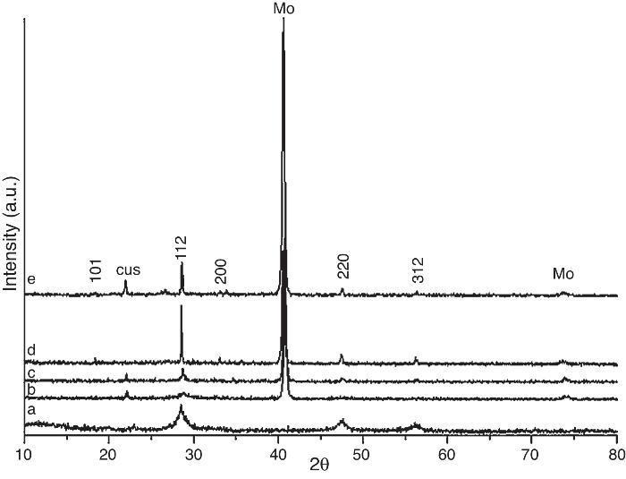
Fig. 1. X-ray diffraction patterns of: (a) as-prepared CZTS powder after solvothermal treatment at 200 °C; (b) CZTS thin film after dry step at 300 °C in a hot plate, (c) CZTS film after thermal treatment at 500 °C, (d) 550 °C and (e) 600 °C after 20 min.
Raman spectroscopy to detect posible secondary phases is required due to the low crystallinity of the as-prepared CZTS powder observed on X-ray measurements.
Fig. 2a shows the plot of spectra intensities versus wave number from Raman spectroscopy measurement for the as-prepared powder.
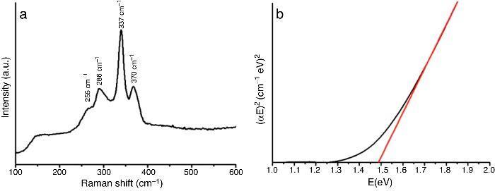
Fig. 2. Spectra of as-prepared CZTS powder using: (a) Raman and (b) UV–vis-NIR spectroscopy.
Three main peaks and a shoulder can be clearly identified. All reflections at 255 cm−1, 286 cm−1, 337 cm−1 and 370 cm−1 can be associated with crystalline CZTS with space group I-42m. No impurities were detected.
UV–vis-NIR measurements show a band gap of 1.49 eV (Fig. 2b). The value is close to that reported in the literature for Cu2ZnSnS4 ([6]). Both band gap and Raman measurements agree with DRX results.
The powder morphology analyzed by SEM shows aggregates of nanoparticles below 100 nm (Fig. 3a). EDX measurements confirm the average elemental composition (Table 1a). Despite the slight lack of S and Sn, the results are close to the initial stoichiometry. Thus, the solvothermal method of synthesis displays good homogeneity and compositional control.
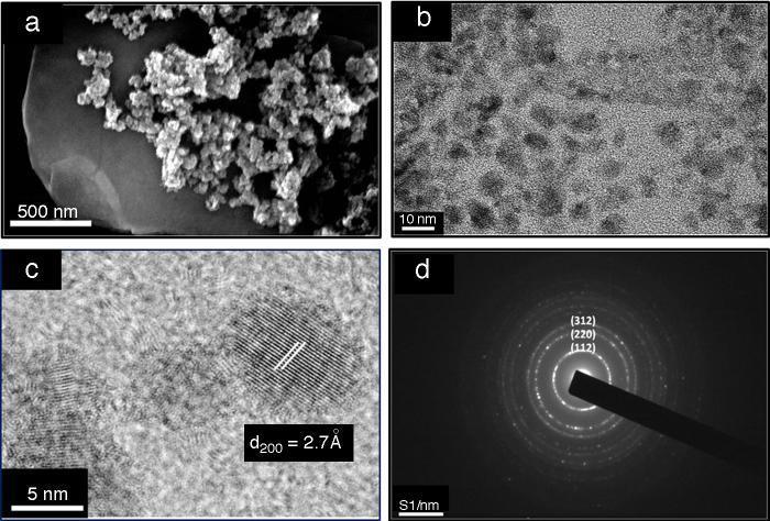
Fig. 3. Images of as-prepared powder after solvothermal treatment using (a) scanning electron microscope (SEM), (b) transmission electron microscope (TEM), (c) closer view of spherical nanoparticles using TEM and (d) selected area electron diffraction (SAED).
Table 1. EDX microanalysis (atomic %) (a) of as-prepared powder and (b) after the thin film thermal treatment at 550 °C 20 min.
| Element | (a) Atomic % | (b) Atomic % |
| Powder | Film | |
| S | 46 | 54 |
| Cu | 26 | 25 |
| Zn | 15 | 11 |
| Sn | 13 | 10 |
Morphology view made by TEM displays nano-sized crystals well dispersed in 1-hexanethiol as a dispersant medium (Fig. 3b). Fig. 3c shows an image of a single particle with elliptic shape; the nanocrystal growth is in the direction of the a axis with (200) lattice planes. Laser diffraction measurement was used in order to obtain the size distribution of the nanocrystals in a high diluted solution of 1-hexanethiol, Fig. 4 shows an average size of about 8.5 nm.
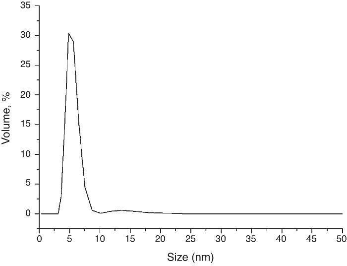
Fig. 4. Size distribution of the nanoparticles using Laser diffraction measurement.
This small average size is due to the use of hexadecylamine as capping agent during solvothermal reaction preventing the crystal growth.
In Fig. 3d electron diffraction pattern is shown, concentric rings in the zero order Laue zone with discrete spots indicative of a polycrystalline material. This fact approves that the material is made up of many tiny single crystals. The continuous rings with discrete reflection spots suggest the existence of crystallites oriented in different preferred directions. From the diffraction rings, the crystallographic planes (112), (220), (312), (008) and (332) were clearly identified.
These results confirm the existence of CZTS as unique phase according to the XRD analysis (Fig. 1a).
CZTS after deposition and drying stepFig. 1b shows the X-ray spectrum after deposition and drying step at 300 °C; the main reflections are mantained. It is worth mentioning that the crystallinity of the as-prepared film must be higher than the powder after drying step. However, initially this fact is difficult to be observed as CZTS signal is masked by the high crystallinity of molybdenum (JCPDS: 00-042-1120). The molybdenum thin film is deposited onto ceramic glaze as a back contact for the future device implement, so it is important to make all the film on this in order to find the best work conditions.
Fig. 5 displays micrographs of secondary electron image of CZTS films. The cross-section image of as-prepared film after drying step (Fig. 5a) reveals a good compacting and adhesion on the substrate, so that a uniform layer with adequate thickness around 2–3 μm is shown. No contrast differences in the CZTS film were detected using backscattered mode. The average size of CZTS particles and the dispersant agent used are important key factors in order to obtain adequate thin films for photovoltaic applications. The desirable thickness of the absorber layer is 2 μm, to avoid electron–hole pair recombination during photovoltaic process. In the photovoltaic device, particles lower than 100 nm are needed to form a thin film of 1 μm in each Doctor Blade deposition with adequate morphology. The tendency of the nanoparticles in dispersion is to join together forming agglomerates; this fact is due to the high energy surface of the nanoparticles, so it is important to use an adequate dispersant. 1-Hexanethiol is widely used in the deposition of nanoparticles ([31]). The sulfur atom in the thiol group of 1-hexanethiol interacts with the nanocrystals recovering the surface and the carbon chain produces steric effect, repealing the other nanoparticles. In addition, 1-hexanethiol has a desirable good adhesion to molybdenum and easy removal in the drying process avoiding cracks on the surface of the absorber layer.
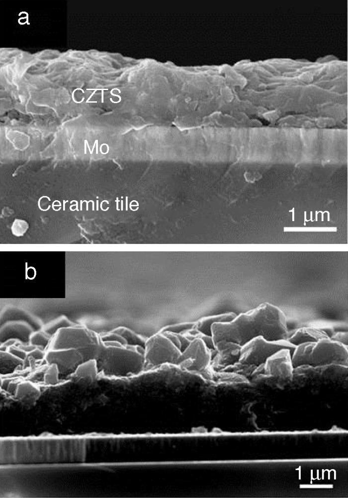
Fig. 5. Cross-section SEM image of (a) as-prepared film after drying step and (b) after thermal treatment at 550 °C 20 min.
CZTS after thermal treatmentIn order to increase the CZTS crystallinity onto ceramic substrate, the sample was treated at 500 °C (Fig. 1c), 550 °C (Fig. 1d) and 600 °C (Fig. 1e). At 550 °C, higher intensity of the kesterite peaks was achieved, free of secondary phases. At 600 °C, loss of crystallinity of kesterite phase during thermal treatment can be observed due to volatility of tin and sulfur. Besides the lack of crystallinity secondary phase of CuS (JCPDS: 03-065-3929) was observed.
Fig. 5b shows the cross-section image of CZTS film after thermal treatment at 550 °C. It can be observed that the formation of large grains on the top of the surface and small grains at the bottom is characteristic of chemical routes. The formation of the large grains is the major responsible of the photoresponse in the photovoltaic devices ([32]); so it is necessary to reduce the small grain layer for the future device implementation.
The thermal treatment was made using an open reactor with small amount of S and Sn in the quartz tube in order to increase their initial lack content in the powder (Table 1a). Compositional confirmation after thermal treatment at 550 °C is shown in Table 1b. The results show slight sulfur increment, comparative to the as-prepared powder, and the lack of small Sn amount was still present. The use of an open reactor does not allow the accurate control of metals and sulfur composition. Because of that, in the next work, the use of a closed graphite box inside of quartz tube ([33]) is planned.
The band gap after thermal treated film at 550 °C remains at 1.5 eV according to Cu2ZnSnS4 formation. CZTS crystal growth onto ceramic tile was realized successfully for the first time.
The future work will focus on finishing the first ceramic photovoltaic tile based on CZTS absorber, after applying buffer and window layer on CZTS structure.
ConclusionsCu2ZnSnS4 powder was successfully synthesized at 200 °C in a solvothermal autoclave using hexadecylamine as a capping agent. Characterization techniques reveal pure kesterite phase of the as-prepared CZTS powder. TEM analysis shows nano-sized crystals with average size of 8.5 nm. The nanoparticles were deposited successfully onto ceramic tile, recovered previously with molybdenum. The morphological study reveals that the obtained coatings are suitable for solar cell applications. Thermal treatment study at different temperatures shows that 550 °C is an optimum temperature to obtain CZTS pure phase with high crystallinity. CZTS crystal growth onto ceramic tile was realized successfully for the first time.
Conflict of interestThe authors have no conflicts of interest to declare.
Acknowledgements
The authors acknowledge the financial support of the Spanish Ministry of Science and Education under INNPACTO (IPT-2011-0913-920000), Reto Investigación (ENE2013-49136-C4-2-R) and Reto Colaboración (RTC-2014-2294-3) programs. We also appreciate the characterization assistance of Central Service of Scientific Instrumentation (SCIC) at the Universitat Jaume I.
Received 21 May 2015
Accepted 16 September 2015
Corresponding author. ivancalvet89@gmail.com