


This paper aims to study the properties of the absorber layer and the heterojunction in kesterite solar cells. The Cu2ZnSnS4 (CZTS) thin films were layered on a glass substrate from a colloidal solution of metal salts and thiourea dissolved in a mixture of water and ethanol and deposited by spin coating technique. The samples were then heat treated in a furnace, in the presence of sulphur powder and under a nitrogen gas flow. The results revealed the formation of homogeneous layers of a pure kesterite phase of CZTS crystallites after heat treatment with correct stoichiometry and oxidation states. The optical transmission measurements indicate an energy band-gap of 1.4eV and an absorption coefficient of 104cm−1. These CZTS thin films, elaborated by spin coating process, were integrated for electronic properties evaluation in a heterojunction in the following configuration: SnO2:F (FTO) and Molybdenum as back contact, CdS as tampon and the CZTS film as absorber layer. The band alignment at the CdS–CZTS heterojunction indicates a cliff-like conduction band offset (CBO) even close to be a flat band.
Este trabajo tiene como objetivo estudiar las propiedades de la capa absorbente y la heterojunción en las células solares de kesterita. Las finas películas de Cu2ZnSnS4 (CZTS) fueron colocadas en capas sobre un sustrato de vidrio a partir de una solución coloidal de sales metálicas y tiourea disueltas en una mezcla de agua y etanol, y depositadas mediante la técnica de revestimiento por centrifugado. A continuación las muestras se trataron térmicamente en un horno, en presencia de polvo de azufre y bajo un flujo de gas nitrógeno. Los resultados revelaron la formación de capas homogéneas de una fase de kesterita pura de los cristales de CZTS después del tratamiento térmico con la estequiometría y los estados de oxidación correctos. Las mediciones de la transmisión óptica indican una brecha en la banda de energía de 1,4eV y un coeficiente de absorción de 104cm−1. Estas películas delgadas de CZTS, elaboradas por el proceso de revestimiento de espín, se integraron para la evaluación de las propiedades electrónicas en una heterojunción en la siguiente configuración: SnO2: F (FTO) y molibdeno como contacto posterior, CdS como tampón y la película CZTS como capa absorbente. La alineación de la banda en la heterojunción CdS-CZTS indica un desplazamiento de la banda de conducción (CBO) similar al de un acantilado, incluso cerca de ser una banda plana.
In recent years, photovoltaic energy has become a promising source for meeting the energy that society demands. Currently, silicon-based solar cells are the most commercialised product on the photovoltaic market. The expensive and polluting manufacturing techniques of crystalline silicon solar cells led scientists to find a new generation of solar cells that are more economical and environmentally friendly.
Thin-film solar cells are a promising alternative that could achieve this goal by reducing the amount of materials. In recent years, three thin-film solar cells technologies were developed: amorphous silicon (a-Si), cadmium telluride (CdTe) and CIGS (CuInxGa1−xSe2). The CIGS technology achieved a higher efficiency (22.9%) than the cadmium telluride (21%) and amorphous silicon (10.2%) [1]. However, (CdTe) technology uses two toxic element (Cd and Te) and the CIGS technology involves the use of rare elements such as indium and gallium. In addition, indium is now widely used in touchscreen technology [2] and its price could significantly increase in the future and affect the production of the CIGS technology.
To avoid the use of toxic and rare elements, new material kesterite (Cu2ZnSnS4 or Cu2ZnSnSe4 referred as CZTS and CZTSe) using copper, zinc, tin, and sulphur or selenium elements, has attracted considerable interest in recent years and became promising for the development of eco-friendly solar cells. This compound is a p-type semiconductor and is therefore used as an absorber layer in solar cells. Its near-optimum direct band gap energy of 1.5eV and its large absorption coefficient, greater than 104cm−1, make it one of the most promising materials for photovoltaic applications [3,4]. Although this innovative technology has grown rapidly in recent years, its performance is weak compared to CIGS. The best efficiency of kesterite solar cells is 12.6% for Cu2ZnSn (S, Se)4 and 10% for Cu2ZnSnS4[1,5].
The development of kesterite solar cells is currently limited by the large open circuit voltage (Voc) deficit [6,7]. This high Voc deficit (Eg/q−Voc) is strongly dependent on several factors, in particular related to the purity of the CZTS absorbent material and the quality and nature of the interfaces between the different layers and non-ideal band alignment that limits charge separation at the absorber/tampon heterojunction [8–10]. Thus, the CZTS layer must be pure (without parasitic phases) and stable during the deposition and the heat treatment processes (no loss of tin and sulphur by evaporation or diffusion in the other layers of the cell). As well as, the heterojunction needs more investigations to understand the recombination limits at the heterojunction-interface absorber/buffer (CZTS/CdS), which is one of the main factors in addition to the absorbent layer problems limiting the efficiency.
Hence, obtaining a pure phase of CZTS required optimisation. The mechanism of formation of secondary phases and decomposition of CZTS phase during heat treatment is still under study [11]. Several authors have reported the presence of secondary phases in the kesterite structure, such as Cu2−xS, SnS, SnS2, Cu2SnS3, which are p-type or n-type semiconductors or insulators, that can form secondary diodes inside of the CZTS [11–13]. A review by Kuma et al. indicates that, under equilibrium conditions, a copper-rich layer can suppress the secondary phases and assist in the formation of the pure phase of CZTS [12]. Kermadi et al. proved that copper-rich CZTS could remove some secondary phases but was unable to remove the copper sulphide phase [14]. Ashfaq et al. recently demonstrated that the use of In2O3:Sn (ITO) substrate promotes the growth of a single-phase, namely CZTS [15]. However, most of the previous studies did not take into account the diffusion mechanisms when using ITO to obtain a single and pure CZTS phase: crystallographically the phase is kesterite but chemically, indium can partially substitute tin and form a Cu2ZnSn1−xInxS4 alloy (CZITS), which may changes the properties of the CZTS and promote the appearance of the In2O3 phase [16].
For the heterojunction engineering, an unoptimised hetero interface between the absorber and the buffer layer could result in a major limitation on device performance. However, the heterojunction engineering has achieved relatively little attention in the kesterite community. Recently, Yan et al. (2018) obtained the efficiency record of kesterite sulphide solar cells by heterojunction heat treatment [5]. Thus, further focused experimental investigations at the absorber-buffer hetero-interfaces will be impactful in the kesterite development.
In this paper, we present the deposition process and the optical, structural, and chemical characterisations of single phase kesterite on a glass substrate by spin coating and sulphurisation process. These CZTS thin films were used in a stack of layers to produce all solution heterojunction. The electronic properties of the CdS/CZTS heterojunction were collected experimentally by XPS including core-level, valance band positions and UV–visible bandgap measurements.
ExperimentalCZTS thin films were deposited on substrates by spin coating and heat treated in a furnace under controlled atmosphere. The complete heterojunction was elaborated using chemical bath deposition and spin coating techniques. Various characterisation techniques were carried out to study the properties of CZTS thin films and heterojunctions.
CZTS thins films preparationThe colloidal solution was prepared by dissolving copper chloride dihydrate, zinc chloride, tin chloride dihydrate and thiourea (H2NCSNH2) with respective concentrations of 0.4M, 0.2M, 0.2M and 1M in a mix of water (75%) and ethanol (25%). Some drops of ethanolamine were added to the solution as stabiliser, where the pH of the solution was around 4. The solution was stirred for 6h at room temperature to obtain a clear yellow-coloured colloidal solution.
CZTS thin films were layered on glass substrates from the colloidal water-ethanol solution by spin coating processing at 4000rpm for 30s. Samples were then dried directly on a hot plate heated at 250°C for 10min under air ambient. This process was repeated 10 times (for a final thickness of 1.2μm). Samples were subsequently heat treated in a furnace at 520°C during 30min in the presence of sulphur (0.5g) under nitrogen gas flow.
Samples CTB01 and CTB01S respectively correspond to the CZTS thin films before and after heat treatment.
Heterojunction fabricationThe heterojunction prototype was built as follows:
- -
The first layer was Molybdenum (Mo). This Mo layer was deposited using an e-beam evaporator (Plassys MEB400) on FTO (fluorine-doped tin oxide, SnO2:F) glass substrates provided by SOLEM Company. The thickness of the Mo layer was 100nm;
- -
The second layer was the CZTS (5 layers) thin film deposited using a spin coating technique as described above (CZTS thins films preparation section);
- -
The third layer was the CdS buffer layer deposited by Chemical Bath Deposition CBD (70°C, 15min). The chemical bath composition was: 20mL of deionised water, 5mL of 0.1M CdCl2, 20mL of 0.1M thiourea and 17.5mL of 6.5M NH4OH. The pH of the chemical bath during the reaction was about 10.
This stack of layers will be referred to as HJ19-01. Finally, a rapid annealing was performed in a furnace at 270°C for 10min under nitrogen gas flow without sulphur. The as-built heterojunction will be labelled as HJ19-01S.
CharacterisationsTransmission Electron Microscopy (TEM) was performed on a JEOL JEM-2100F microscope to characterise the CZTS thin film microstructure. For the preparation, thin films were removed from the substrate by scratching them with a scalpel. Afterwards, the sample surface is wiped with a carbon-coated gold grid, resulting in pieces of the films stuck to the carbon film. The local morphology and the crystallography were studied using conventional, high resolution microscopy (HRTEM) and Selected Area Electron Diffraction (SAED) modes.
The surface morphology (Plain view) and the multilayer stack (cross-section) of the heterojunction were examined by Scanning Electron Microscopy (SEM). The observations were performed on a Hitachi SU8230 SEM equipped with an Energy Dispersive Spectrometer (Thermo Scientific NSS SDD) allowing chemical analyses of the films.
The atomic states, chemical compositions and valence band data were determined by X-ray Photoelectron Spectroscopy (XPS) and performed using a PHI Versaprobe 5000 apparatus with monochromated Al Kα1 X-rays (energy of 1486.6eV, power of 50W and X-ray spot diameter of 200μm). Experiments were realised after sputtering of the CTB01, CTB01S and HJ19-01S samples in order to remove the major part of the thin layer of oxide from atmospheric contamination. Sputtering was done with argon ions of 500eV for 5min for the thin films (incidence angle of 45°). For the heterojunction, the XPS data were collected after each 60s of etching time. In this condition, the sputtering rate of standard silicon dioxide is around 2nm/min. Adventitious carbon from atmospheric pollution is used as internal standard for energy calibration (1s level at 284.8eV). During measurements, the residual pressure of the analysis chamber was maintained below 10−7Pa. Spectra were processed with the Casa software package and the ionisation cross-sections from Landau model were used in order to quantify the semi-empirical relative sensitivity factors.
The crystallographic structures of samples was investigated by X-Ray Diffraction (XRD) and performed with a Bruker D8 DISCOVER (CuKα radiation source λ=1.5406Å).
The size of nanocrystals was estimated from the Scherrer formula [17]:
where λ is the X-ray wavelength used, Bhkl the full width at half maximum and θ the Bragg angle of the studied peak.
The Raman spectroscopy (Raman) was performed with a custom-built epi-confocal microscope equipped with a 40× objective lens (0.6 NA, Nikon). The sample was illuminated with a laser excitation wavelength of 784nm and an intensity of 0.6mW at the focus. Raman spectra were acquired with a spectrometer (equipped with a grating of 1200 lines/mm) associated with a cooled CCD camera (1024×256 pixels). An exposition time of 10s was used and the calibration was performed using a (111) silicon wafer at 520cm−1.
The Ultraviolet–visible Spectroscopy (UV–vis) was performed with a Thermo Spectronic Helios Gamma spectrophotometer, in the wavelength range 190–1100nm with a 0.5nm step to record the transmittance of thin films and to calculate the absorption coefficient, α, from the following equation:
where e is the film thickness and T the transmittance [18]. Noted that the film thickness was measured using a Dektak 6M Profilometer (Veeco).
The optical band gap values were determined using the Tauc diagram [16] where (αhυ)2 is plotted as a function of the energy hυ. The value of the gap is that at the intersection of the extrapolation of the linear part of the curve with the abscissa axis.
Results and discussionCrystallographic and chemical characterisationThe XRD diffractogram of the CZTS layer before heat treatment (CTB01) is showed in Fig. 1a. The three major peaks at 28.43°, 47.27° and 56.15° are respectively assigned to the (112), (220) and (312) crystallographic planes of the kesterite tetragonal structure of CZTS (PDF card #04-015-0223). In addition to the CZTS major phase, the SnO2 cassiterite phase is also detected, see peaks (110), (101) and (211) at respective angles 26.49°, 33.77° and 51.72° (PDF card #04-003-0649). This SnO2 phase emerges during the drying process in ambient air on the hot plate.
 raw sample CTB01, (b) heat treated sample CTB01S.")
The size of the nanocrystals, derived from the Scherrer formula, varies from 5.5nm to 8.8nm for each peak.
The XRD pattern of the annealed CZTS layer, CTB01S (Fig. 1b) shows narrow and intense diffraction peaks corresponding to the pure kesterite CZTS structure without secondary phase. The cassiterite peaks have disappeared during annealing. Tin dioxide can turn into solid tin monosulphide [19,20] during annealing under sulphur atmosphere and tin monosulphide is a volatile specie above 500°C [21].
The size of the nano-crystallites varied between 18.7nm and 23.1nm depending on the chosen peak. The peak intensities highlight an isotropic growth of the crystallites. Logically, the crystallites size increases under heat treatment.
The heat treatment under sulphur and nitrogen gas flow (oxygen free) prevents the formation of oxidised phases, increases the crystallisation, and helps the formation of the CZTS kesterite phase. In some case, as it seems to be the case here, it also avoids the decomposition of this structure into binary and ternary compounds such as Cu2−xS, SnS2, ZnS, Cu2SnS3 which has been observed by several authors in the literature [11–13].
In order to confirm the absence of secondary structures (as ZnS and Cu2SnS3, for which the three mains X-ray diffraction peaks are identical to CZTS ones), the SAED technique, the Fast Fourier Transformation of HRTEM image and the Raman spectroscopy were complementary performed.
Fig. 2(a, b) shows one electron diffraction patterns and the Fast Fourier Transformation of a High-Resolution image (HRTEM) of sample CTB01. The calculation of d spacing (Table 1) from the SAED confirm the results of XRD. Only pure Cu2ZnSnS4 kesterite crystallites were found in the studied samples. Fig. 2c shows where the SAED at the chemical analysis (EDS) were performed. The chemical composition in this area (Fig. 2d) shows the presence of four elements of the CZTS compound: copper, zinc, tin, and sulphur.
 Selected area electron diffraction pattern of the area shown in image (c); (b) fast Fourier transformation of a high-resolution image (HRTEM); (c) area of SAED and EDS acquisition; (d) energy dispersive spectroscopy (EDS) spectrum of image.")
d-Spacing calculated from the selected area electron diffraction (SAED) and the associated diffraction planes.
Fig. 3a shows the Raman spectrum of the CTB01 sample. The strongest peak at 335cm−1 corresponds to the A mode of the kesterite structure of CZTS which is theoretically reported by Gurel et al. [22]. The weak peak at 363cm−1 is assigned to the E (LO) mode of kesterite structure of CZTS [23]. For the calcined CTB01S sample (Fig. 3b), the peaks at 287cm−1 and 337cm−1 are assigned to the two A modes of the kesterite structure as well as the peaks at 366cm−1 and 373cm−1 which corresponds to the E(LO) and B(LO) modes [24–26]. The new intense peak at 287cm−1, may due to a better crystallinity of CTB01S compared to CTB01. As no other peaks are observed neither the ZnS (at 348cm−1) nor the Cu2−xS (at 476cm−1), SnS2 at (315cm−1) and Cu2SnS3 (at 352cm−1) phases are present [27–32].
 As deposited sample CTB01, (b) heat treated sample CTB01S.")
The different oxidation states were measured by XPS before and after etching for the CTB01 and CTB01S samples (see Fig. 4).
 Cu2p, (b) Zn2p3/2, (c) Sn3d5/2 and (d) S2p.")
XPS spectra in Fig. 4a show the binding energy of Cu 2p3/2 and Cu 2p1/2 core levels, respectively at around 932 and 952eV, for the raw and annealed CZTS samples. The measured binding energy for the Cu 2p3/2 level and the absence of satellite at high binding energy for both peaks corroborate the Cu(I) oxidation state of copper in the whole CZTS layers [33–35].
The binding energy value of about 1021.8eV for Zn 2p3/2 core level confirms the presence of Zn(II) for both CZTS layers, before and after calcination (see Fig. 4b) [35].
The Sn 3d5/2 level for CTB01 and CTB01S samples are shown in Fig. 4c. Energy of this level slightly above 486eV confirms the presence of Sn4+ species in the two samples [35,36].
Fig. 4d shows the XPS results for the sulphur species. The 2p3/2–2p1/2 doublet could be separated in two distinct peaks: one centred near 162eV, the other near 163eV. The component at high binding energy 168eV corresponds to sulphate SO42− which decreases during sputtering but still detected after sputtering. The bulk component at low energy is assigned to the S2− sulphur specie [37].
The chemical composition was also determined by EDS analyses for CTB01 and CTB01S samples (Table 2). The theoretical atomic composition of CZTS samples is respectively 25, 12.5, 12.5 and 50 percent for copper, zinc, tin and sulphur. The ratio Cu/(Zn+Sn) remains close to 1 for both samples and is the stoichiometric expected value. On the other hand, the S/(Cu+Zn+Sn) ratio of about 0.4 for sample CTB01 is very low compared to the theoretical one of 1. This could be due to the evaporation during the drying process after each deposition cycle. This ratio increases almost to 0.9 after annealing. This indicates that annealing under sulphur atmosphere allows to fill the sulphur vacancies and reach the Cu2ZnSnS4 stoichiometry.
From XPS analysis we can conclude that Cu(I), Zn(II), Sn(IV) and S(-II) are present in each sample. The formula Cu2ZnSnS4 is then consistent with XPS analysis and atomic concentrations obtained by EDS.
In conclusion, there is a good match between XRD analysis, electronic diffraction, Raman measurements, XPS analysis, and Energy Dispersive Spectroscopy which indicate the achievement of near stoichiometric CZTS of pure kesterite phase and required oxidation states.
Microstructural characterisationFig. 5(a–d) shows SEM images of the top view of CZTS thin films before CTB01 and after CTB01S heat treatment with different magnifications. Fig. 5(a, b) at low magnification (3000×) show a homogeneous surface without cracks for both CTB01 and CTB01S samples. Fig. 5(c, d) are at higher magnification (30000×). CTB01S shows a larger grain size compared to CTB01.
 As deposited sample CTB01, (b–d) after heat treatment sample CTB01S. (e) SEM cross-section image of the heterojunction prototype HJ1901S. (f) EDS analysis across the heterojunction HJ1901S (in scanning TEM mode).")
Fig. 5(e–f) shows the SEM cross-section image of sample HJ19-01S and the corresponding EDS spectra of the different layers of the stack but acquired in STEM-EDS mode. New configuration was used to fabricate the heterojunction by employing FTO/Mo as a back contact (Heterojunction fabrication section). This new design allows to reduce the thickness of interfacial layer MoS2 during heat treatment. In fact, a relatively thick layer of MoS2 forms a Schottky-type barrier and favourite the decomposition of absorber layer in CZTS solar cells [18,6].
According to the SEM image, the thickness of the back contact is approximately 400nm for FTO and 150nm for Mo/MoS2. The thickness of the absorber (CZTS) and the buffer (CdS) are almost 560nm and 90nm respectively. In the absorber layer, we notice the existence of two layers of different morphology: one with large grains on the bulk side and the other with smaller grains on the surface side of the CZTS. This last layer is close to the CZTS-CdS interface. According to the EDS analysis in Fig. 5(f) this variation due to the diffusion of Cd into the CZTS absorber layer.
Optical measurementsFig. 6a shows the transmittance spectrum of CZTS samples before (CTB01) and after (CTB01S) heat treatment. The curve indicates that both layers have a low transmittance in the range 200–1100nm, which mean high photons absorption by the CZTS layers. In addition, over the area 300nm to 400nm and 800–1100nm, the transmittance for CTB01S is higher than CTB01. However, above 450–800nm the transmittance decreases for the heat-treated sample CTB01S.
 Transmittance of the CZTS thin films; absorption coefficient of the CZTS thin films as a function of energy, (b) as deposited sample CTB01, (c) sample after heat treatment CTB01S; optical band gap of the CZTS thin films (d) CTB01 and (e) CTB01S.")
Fig. 6(b–e) shows the band gaps and absorption coefficient as a function of energy for the two samples CTB01 and CTB01S. The band gap of CTB01 is about 1.5eV and the absorption coefficient is estimated to be 3.3×104cm−1 at 1.5eV and 5.8×104cm−1 at 3eV. The band gap of CTB01S decrease after heat treatment to be 1.4eV, the absorption coefficient at this value was estimated to be 2.8×104cm−1 and 5.6×104cm−1 at 3eV. However, there is a second optical transition below the bandgap for both samples, which may due to tail states [38,39].
As results, the absorption coefficient of 104cm−1 and the band gap range of about 1.4eV to 1.5eV for the heat-treated layers CZTS make these films suitable to be incorporated as an absorber layer for thin films solar cells. This is consistent with several theoretical and experimental studies [3,4,40].
Heterojunction engineeringThe electronic characterisation of CdS/CZTS heterojunction was determined from XPS depth profile measurements including valence band (VB) and core level (CL). A low-energy argon sputtering was applied from the upper CdS layer to the lower CZTS layer passing through the hetero-interface. In this way it is possible to access the values of core level energy used to determine the band bending (Vbb) both in bulk and at the interface. Based on Kaut formula shown in Eq. (1)[41–43], the (Vbb) value equals to 0.42eV.
where ECLa and ECLb are the core level energies of two selected elements in the CdS and CZTS bulk respectively, ECLai and ECLbi are the same core level energies measured at interface.
Measurements on VB region are done between −1 and 7eV (assuming BE at 0eV represent the energy of fermi level energy Ef and the bending energy below 0eV was negative) for pure CdS (Fig. 7a) and pure CZTS (Fig. 7b). The VB positions were estimated by extrapolation of the linear slope in the VB spectra near Ef. In this way the VB position of the bulk materials are about −1.75eV for CdS and −0.24eV for CZTS.
 and CZTS(b). (c) Band alignment at CdS–CZTS heterojunction.")
The band alignment at the heterojunction, was estimated using the indirect method by applying the valance band offset (VBO) and Conduction band offset (CBO) values. The VBO was deduced from the VB positions and the band bending as shown in Eq. (2). The CBO was calculated by adding the optical band offset of CdS–CZTS to the VBO value as indicated in Eq. (3).
where EbVB and EaVB represent the valence band energy of CZTS and CdS respectively.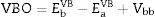
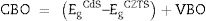
Fig. 7c shows the band alignment at CdS–CZTS heterojunction where VBO is about −1.09eV and CBO about −0.09eV which indicate small cliff like CBO close to be flat band. These results indicate good alignment of the heterojunction CdS–CZTS, which can improve the efficiency of pure sulphide Kesterite devices.
ConclusionCZTS thin films were successfully deposited by spin coating from a colloidal solution. The characterisation results show that the CZTS thin films deposited by spin coating and sulphurised at 520°C with solid sulphur under nitrogen ambient, are of pure kesterite structure of Cu2ZnSnS4 with the proper oxidation states. The optical band gap of 1.4eV and the absorption coefficient greater than 104cm−1 seem ideal for an absorbent layer in solar cells.
The heterojunction indicates a good band alignment by heat treatment of the heterojunction which indicates a cliff like CBO even close to being a flat band. As a result, it can facilitate charge separation and improve the efficiency of pure sulphide kesterite devices.
This work has been supported by the Algerian Ministry of Higher Education and Scientific Research MESRS, Campus France, CAKE BQR ICB project and EIPHI Graduate School (contract ANR-17-EURE-0002).