


Al-doped zinc oxide (ZnO) films were deposited on glass substrates by radio frequency magnetron sputtering using a sintered target of nanoparticles synthesized by sol–gel. The films were characterized using X-ray diffraction, scanning electron microscopy, the four-point probe method for resistivity, energy dispersive X-ray spectroscopy and photoluminescence. The X-ray diffraction patterns showed a hexagonal structure corresponding to the wurtzite phase for all the films, nanoparticles, and sintered targets. The films deposited by sputtering showed a highly preferred orientation to the (002) plane. These films were compared structurally and electrically to those deposited by the sol–gel method. Photoluminescence spectra show a decrease in intensity due to the reduction of defects by the incorporation of Al as dopant in the ZnO films deposited by the both methods (sol–gel and sputtering). The Al-doped ZnO films deposited by sputtering reached resistivity of 0.1Ωcm and those deposited by sol–gel reached a resistivity of 1.24Ωcm. The physical properties of these films show potential for application in devices like sensors and biosensors.
Se depositaron películas de óxido de zinc (ZnO) dopadas con aluminio (Al) sobre sustratos de vidrio mediante erosión catódica de radiofrecuencia usando un blanco sinterizado de nanopartículas sintetizadas por sol-gel. Las películas fueron caracterizadas usando difracción de rayos-X, microscopía electrónica de barrido, método de cuatro puntas para la resistividad, espectroscopía de energía dispersiva de rayos-X y fotoluminiscencia. Los patrones de difracción de rayos-X mostraron una estructura hexagonal correspondiente a la fase wurtzita para todas las películas, nanopartículas y blancos sinterizados. Las películas depositadas por erosión catódica mostraron una alta orientación preferencial al plano (002). Estas películas fueron comparadas con las depositadas por el método sol-gel, estructural y eléctricamente. Los espectros de fotoluminiscencia muestran una reducción en intensidad debido a la reducción de defectos por la incorporación de Al como dopante en las películas depositadas por ambos métodos (sol-gel y sputtering). Las películas de ZnO dopadas con Al depositadas por erosión catódica alcanzaron resistividades de 0,1 Ω cm y 1,24 Ω cm para las películas de ZnO dopadas con Al depositadas por sol-gel. Las propiedades físicas de estas películas muestran potencial para la aplicación en dispositivos como sensores o biosensores.
Zinc oxide (ZnO) is an intrinsic n-type semiconductor of the II–VI family; it has a 3.37eV direct transition band gap and an exciton binding energy of 60meV at room temperature. ZnO has high transmittance in the visible region. ZnO normally occurs in a hexagonal wurtzite-type structure classified in the P63mc space group with lattice parameters a=b=3.249Å and c=5.2042Å with a relationship c/a=1.602 [1–3]. Some of these properties of ZnO can be adjusted by doping. Commonly, ZnO is doped with Gallium (Ga), Indium (In), or Aluminum (Al), which are the elements of group III that are the most used to improve the electrical and optical properties of ZnO. However, the precursors of Ga and In are usually more expensive than the precursors of Al. Consequently, doping with Al may be an alternative for obtaining good physicochemical properties using low doping percentages. Aluminum is an efficient n-type dopant that reduces oxygen vacancy defects; these defects impact the stability of resistivity [2]. Photoluminescence can provide some important information related to the surface defects and oxygen vacancies, and energy levels in semiconductor materials like ZnO. Wang et al. mention that Al incorporation induces changes in energy levels and modify oxygen concentration, so photoluminescence is an adequate technique to analyze the effect of Al as a dopant in ZnO [4].
ZnO is a highly studied material that has different applications. It is used to promote growth in plants when added as nanoparticles [5]. It is used in biomedical applications [6], and as a photocatalyst material [7,8] in devices such as photovoltaic cells, liquid-crystal display (LCD) screens, diodes, ultraviolet (UV) lasers, and sensors [9–15]. ZnO is a convenient material for biosensor design because it can be inexpensive and biocompatible, and it enables devices to have a large surface area, high catalytic capacity, and high electron transfer rate. As a consequence, this material has been used successfully for the detection of glucose, cholesterol, urea, uric acid, vitamins, neurotransmitters, amino acids, captopril [16–19], non-enzymatic glucose sensors [20], and dopamine [21], among others.
ZnO can be synthesized as nanoparticles, thick films, and thin films. However, ZnO films offer the advantage that the material can be recovered easily after use, and they take advantage of the electrical properties of ZnO on a large scale. The techniques used to deposit ZnO films for application in solar cells, sensors, and other devices are screen printing [22–24], chemical bath [25–27], successive ionic layer adsorption and reaction (SILAR) [28,29], drop-casting [30], sol–gel, and sputtering. The sol–gel technique has the advantage that it can produce thin films with low resistivity and high surface area by adjusting the deposit conditions.
On the other hand, the sputtering technique deposits ZnO films onto substrates directly, without the need for subsequent heat treatment, which facilitates the coating of different surfaces such as polyethylene terephthalate (PET), glass, and quartz without compromising their physicochemical properties, as the obtained films have a highly crystalline quality and low resistivity. Many studies use commercial targets for the sputtering process, or manufacture targets by compressing commercial ZnO and Alumina (Al2O3) powders [31–33]; this implies that the doping occurs during the sputtering process. However, some studies use targets synthesized using a chemical process [34], such as sol–gel. These targets have the advantage that during the powder obtention, the doping agent is present inside the lattice before the sputtering process.
In this study, the physicochemical properties of ZnO nanoparticles, and ZnO nanoparticles doped with Al obtained by the sol–gel process were analyzed. In addition, we carried out a comparative study of the structural, electrical and photoluminescence properties of ZnO and ZnO doped with Al (AZO) films deposited on glass, obtained by sol–gel and by sputtering using synthesized targets obtained from the powders derived from the sol–gel process.
Experimental procedureMaterialsThe reagents used were zinc acetate dihydrate (ZAD, Zn (CH3COO)2·2H2O) of analytical reagent (AR) quality from Sigma–Aldrich (India) and aluminum nitrate nonahydrate (Al (NO3)3·9H2O) of AR grade, from Sigma–Aldrich (Germany). Ethanol was used as a solvent. Diethanolamine (DEA, NH(C2H4OH)2) was used as a stabilizer.
Synthesis of nanoparticles and target preparation for sputteringZAD was added to a solution of DEA and ethanol at 50°C under stirring, and Al (NO3)3·9H2O was added as the aluminum doping agent. The final solution presented a concentration of 0.5M of ZAD. DEA was maintained at a molar ratio of 1:1 with respect to ZAD. The concentration of the dopant was fixed at a 1% molar percentage of Al3+ with respect to Zn2+ (Al3+/Zn2+). The precursor solution was aged for 10 days and dried at the boiling point until the solvent in the sample was completely evaporated. Subsequently, the product was calcined at 300°C for 30min. Thermal treatment was carried out at 500°C for 1h to remove the organic remnants and to allow the nanoparticles to completely form.
For the ZnO nanoparticles synthesis, the process and thermal treatment were the same as described above for the AZO nanoparticles, but without adding the doping agent (Al (NO3)3·9H2O).
The resulting nanoparticles powders were pressed using a 2½-in. die with a pressure of 16MPa and then sintered at 1000°C for 1h using a 5°C/min heating ramp. The sintered target was used to obtain films using radio frequency (RF) magnetron sputtering.
AZO and ZnO films deposited by sputteringThe films were deposited on glass slide substrates (corning slides) using RF magnetron sputtering (Intercovamex V3). The substrates were cleaned with liquid soap, rinsed with distilled water, rinsed with ethanol, and placed in an ultrasonic bath using a mixture of acetone, xylene, and ethanol in a ratio of 1:1:1 by volume for 30min. Finally, the substrates were rinsed with acetone and dried. The powers used during the deposit were 100 and 150W, and the power densities were 3.785W/cm2 and 5.677W/cm2, respectively. The substrate temperature was kept constant at room temperature. The argon (Ar) pressure was kept constant at 2×10⁻²mbar with a flow of 180 standard cubic centimeters per minute (sccm). The distance between the substrate and the target was maintained at 7cm. The procedure and parameters for depositing the ZnO and AZO films were the same.
AZO and ZnO films synthesized by sol–gel/dip-coatingZAD was added to a solution of DEA with ethanol at 50°C under stirring, and Al (NO3)3·9H2O was added as the doping agent. The final solution was a concentration of 0.5M ZAD, and DEA was maintained at a molar ratio of 1:1 with ZAD. The concentration of the dopant was fixed at 1% the molar percentage of Al3+ with respect to Zn2+ (Al3+/Zn2+). The precursor solution was aged for 10 days, and the films were deposited on glass slide substrates using the dip-coating technique with a withdrawal speed was 6cm/min, and then dried at 300°C for 15min in an air atmosphere. To obtain films with adequate thickness, the dipping-drying process was repeated seven times. Afterward, the films were sintered at 530°C for 1h.
ZnO films were deposited using the process and thermal treatment described above for the AZO films, but without adding the doping agent (Al (NO3)3·9H2O.
Characterization techniquesTo determine the crystal structure, thin films were characterized by X-ray diffraction using a Rigaku Dmax2100 (Cu kα radiation, λ=1.5405Å) diffractometer. From the X-ray diffraction patterns, the crystallite size was calculated using the Debye–Scherrer equation [35]:
where k is the Scherrer constant, β is the full width at half maximum (FWHM), λ is the wavelength of the X-rays used, and θ is the angle at which the refraction takes place. This analysis was performed using JADE software and with consideration for the standard Si diffraction pattern in the adjustment of the calibration curve.
Similarly, the texture coefficient (TChkl) was calculated using the Harris texture equation [35,36]:
where Ihkl is the experimental intensity, Iohkl is the reference intensity obtained from a powder diffraction file (PDF), and N is the number of planes considered for the analysis.
The morphology of the films was obtained by field emission scanning electron microscopy (FE-SEM) at 1.0kV for nanoparticles and 2.0kV for films. The detector was a secondary electron (SE) detector (JEOL 7610F). From the FE-SEM images collected, the size of the grains in the thin films and the particle size of the powders synthesized from sol–gel were determined using ImageJ software, and the results are reported as mean±standard deviation. The size of the AZO nanoparticles was measured longitudinally. The thickness measurement was carried out using a 3D interference profilometer (optical profilometer, Bruker-Contour GT-InMotion 3D). The resistivity measurement was carried out using the four-point probe method (Loresta-6P equipment, model MCP-T600). The semi-quantitative analysis was carried out with energy dispersive X-ray spectroscopy (EDS) using an environmental scanning electron microscope (ESEM, Philips XL30). Photoluminescence spectra for ZnO and AZO films were measured at room temperature using an LS-55 spectrophotometer (Perkin Elmer, Waltham, MA, USA). The samples were excited at 325nm and the spectrum was collected in the wavelength range of 350–600nm.
Results and discussionAZO nanoparticles and target for sputteringFig. 1A shows the X-ray diffraction pattern corresponding to the nanoparticles obtained by the sol–gel method for AZO and ZnO. The patterns agree with the wurtzite phase according to PDF 36–1451, which describes this phase as a hexagonal structure. The average crystallite size for the AZO nanoparticles is 64nm, and for ZnO, it is 68nm.
 ZnO nanoparticles and AZO nanoparticles, (b) AZO target and ZnO target for sputtering.")
The X-ray diffraction patterns of the sputtering targets are presented in Fig. 1B for AZO and ZnO. In both instances, a random orientation agrees with the PDF. The analysis of the X-ray diffraction patterns does not show impurities like aluminum oxide. After pressing and sintering the nanoparticles, the average crystallite size grew to 86nm for the AZO target, and to more than 100nm for the ZnO without doping. This increment in crystallite size is due to the diffusion process in the solid or semi-solid state in which sintering is carried out. After the sintering process, the target diameter changed from 6.35cm (2.5in) to 5.08cm (2in), therefore, the diameter was reduced by 20% for both targets (AZO and ZnO), and the density reached was 93% of the theoretical density for AZO and 95% of that for ZnO (ZnO theoretical density is 5.675g/cm3[37]).
In Fig. 2, the FE-SEM images and the size distribution of the synthesized nanoparticles are presented. The FE-SEM images show semispherical particles of ZnO without doping (Fig. 2a) and rod-like particles of AZO (Fig. 2b). In Fig. 2c, the size distribution of ZnO nanoparticles is presented: the mean size is 45±18nm. In Fig. 2d, the size distribution of the AZO nanoparticles is presented: the mean size is 123±75nm. The incorporation of Al as dopant during the nanoparticle synthesis modified the morphology and the size distribution, as presented in the figure. The effect of Al on the morphology of AZO nanoparticles has been previously reported by Rameshkumar et al. In their work, they synthesized AZO nanoparticles using the co-precipitation method, and they obtained rod-like particles in the range of 1–2μm [7]. All of these results show that the incorporation of a small amount of Al impacts the morphology of the nanoparticles.
 ZnO and (b) AZO; size distribution for (c) ZnO particles and (d) AZO particles.")
The wide distribution of particle sizes, presented at the bottom of Fig. 2 for both systems, shows the growth in crystallite size calculated for the sintered targets. Considering the presence of particles of 10nm size and the grain boundary diffusion, it is evident the mass of the smaller particles diffuses better than that of the larger particles, according to a process known as the coarsening of particles [38].
The FE-SEM image of the ZnO target (Fig. 3a) shows grains of different sizes, in the range of 25–1000nm. The size distribution presented in Fig. 3c evidences the broad range, there are two different grain size, the first mean size centered at 73±24nm and the second mean size was 750±400nm. The FE-SEM image of the AZO target is presented in Fig. 3b. It shows grains bigger than 700nm and smaller than 100nm. The size distribution presented in Fig. 3d shows a broad range, but the mean size was 270±200nm. The broad standard deviation for both systems (ZnO and AZO) was obtained due to the different grain sizes seen in the FE-SEM images. Moreover, the morphology, size, and distribution of particle size explain the higher density of the ZnO target compared with the AZO target. The arrangement of particles previous to and during the sintering process was favorable to the greater densification of ZnO, this is evident in the FE-SEM images of the targets.
AZO and ZnO films ZnO target and (b) AZO target; size distribution for (c) ZnO target and (d) AZO target.")
Fig. 4 shows the X-ray diffraction patterns of AZO films deposited by sol–gel (A and B), and by sputtering (C, D, and E). There is a difference between the X-ray diffraction patterns of the films deposited using the two techniques.
 ZnO and (b) AZO; by sputtering (c) ZnO at 100W, (d) AZO at 100W, (e) AZO at 150W.")
The X-ray diffraction patterns show a random orientation of the crystalline structure according to PDF 36–1451 for the films deposited by sol–gel. For the films deposited by sputtering at 100W and 150W, the X-ray diffraction patterns show a pronounced peak around an angle of 34 degrees, indicating a preferential orientation to the (002) plane. The absence of additional peaks in the AZO thin film X-ray diffractograms indicates that no other impurities, such as aluminum oxide, were formed.
The FE-SEM images show the early effect of the addition of aluminum on the morphology of the particles, but there is no presence of Al2O3 or any other secondary phase in the X-ray diffraction patterns. This implies that Al gets into the crystalline structure, as previously reported [34,39].
The texture coefficients (TCs) for the thin films are presented in Fig. 5. For thin films deposited by sputtering, the TC shows a preferential orientation to the (002) plane; however, thin films deposited by sol–gel present a low orientation in the same plane.

The preferential orientation presented for the thin films deposited by sputtering can be explained by the drift model and the surface energy. The drift model indicates that nucleation at different planes is carried out in the first stages of the deposit of the film, and the nuclei that survive the competition are those that grow fastest on the substrate [35,40]. Furthermore, the (002) plane is the one with the lowest free surface energy, which is why growth in that direction is favored [36]. In addition, for the thin films deposited by sputtering, the values of TChkl increase with increasing power (Fig. 5).
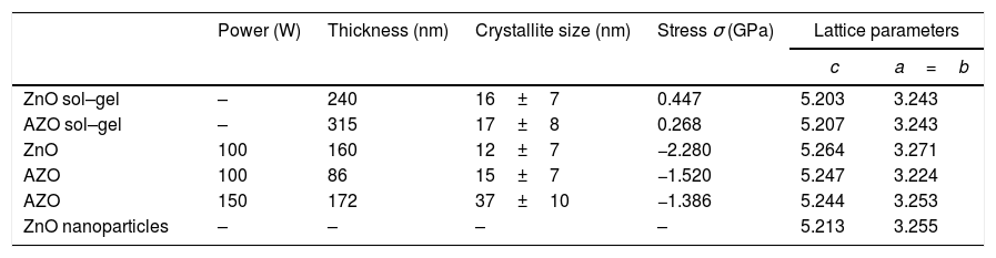
Table 1 shows the lattice parameters calculated from the X-ray diffraction patterns, crystallite size, and in-plane stress (σ). Considering the biaxial strain model and the elastic stiffness constants for the ZnO, the equation can be written as [41]:
Properties of films obtained by sputtering and sol–gel. Thickness, crystallite size, in-plane stress, and lattice parameters.
| Power (W) | Thickness (nm) | Crystallite size (nm) | Stress σ (GPa) | Lattice parameters | ||
|---|---|---|---|---|---|---|
| c | a=b | |||||
| ZnO sol–gel | – | 240 | 16±7 | 0.447 | 5.203 | 3.243 |
| AZO sol–gel | – | 315 | 17±8 | 0.268 | 5.207 | 3.243 |
| ZnO | 100 | 160 | 12±7 | −2.280 | 5.264 | 3.271 |
| AZO | 100 | 86 | 15±7 | −1.520 | 5.247 | 3.224 |
| AZO | 150 | 172 | 37±10 | −1.386 | 5.244 | 3.253 |
| ZnO nanoparticles | – | – | – | – | 5.213 | 3.255 |
where C is the lattice parameter calculated for the film and Co is the lattice parameter of reference. The Co used as a reference is the lattice parameter calculated for the ZnO synthesized nanoparticles. A negative sign for σ indicates that the films present compressive stress. In contrast, a positive σ for the ZnO and AZO thin films deposited by sol–gel indicate tensile stress. The AZO films deposited by sol–gel show tensile stress (0.268GPa), in contrast to the films deposited by sputtering at 100W, which present compressive stress (−1.520GPa). The AZO films deposited by the sputtering process at 100W show tensile stress of −1.52GPa, a smaller magnitude than that of ZnO films (−2.28GPa) deposited under the same conditions. This is because the ionic radius of Al3+ (0.053nm) is smaller than that of Zn2+ (0.074nm), considering that according to Singh et al., Al3+ enters the crystal lattice at substitutional sites [39]. The compressive stress is also associated with crystal defects caused during the deposition of the films. The compressive stress decreases with the increasing deposition power of the ZnO films doped with Al. This behavior has been reported before for ZnO films [40,42].
The FE-SEM images shown in Fig. 6 are evidence that the films deposited by sol–gel present pores, a characteristic of the sol–gel technique due to the surface tension during the removal of the solvent and the formation of grains during the drying and sintering process. The grain sizes are 26±10nm and 51±16nm for the ZnO and AZO, respectively. The addition of Al as Al (NO3)3·9H2O changes the properties of the precursor solution; it can act as an additive, affecting the hydrolysis and condensation by increased water concentration and modifying the grain size in the films [43].
 ZnO, (b) AZO; sputtering (c) ZnO at 100W, (d) AZO at 100W, (e) AZO at 150W and (f) grain size for thin films deposited by sol–gel and sputtering (bar represents standard deviation).")
The films deposited by sputtering do not present pores, and the grain size of the AZO films elaborated by the sputtering process at 100W is 35±12nm, whereas the film deposited at 150W has an average grain size of 58±13nm. Both are smaller than the grain size of the undoped ZnO films deposited by sputtering (66±33nm). The large standard deviation of the grain size distribution of ZnO films deposited by sputtering indicates the presence of small grains (<20nm) and large grains (>100nm). This can be seen in the FE-SEM image, and the size of many grains is between 40 and 80nm. However, the narrower grain size distribution of the AZO films might have been associated with the addition of the dopant under the same deposit conditions. The smaller grain size can be attributed to an effect of Al, because doping can limit the grain growth during film deposition, considering the modeling of grain growth in impure systems [44].
In Fig. 7, the EDS analysis shows that the Al is present in the thin films deposited by both methods. The Al content of approximately 0.8% (Al/Zn) in the films deposited by sol–gel could be due to the measurement technique, considering that EDS is a semi-quantitative analysis, and the Al content obtained is acceptable compared with the calculated in the preparation of the precursor solution.
 Representative EDS of the target of AZO, and (B) EDS analysis for the aluminum content for the thin films and the ZnO in bulk.")
In the films deposited by sputtering, the aluminum content also increases with the power increase. For both power levels, the content of Al is higher than that of the target. Similar results have previously been reported [45,46]. This can be explained considering that the binding energy is higher for Al–O than for Zn–O, and the collision of the plasma with the substrate promotes the deposition rate for Al over that for Zn [45].
The room temperature photoluminescence spectra of ZnO and AZO films deposited by the sol–gel method are in Fig. 8a. The room temperature photoluminescence spectra of ZnO and AZO films deposited by sputtering are in Fig. 8b. The samples were excited at 325nm. There are significant bands in the range of 390–398nm (UV emission); there are also bands in the range of 410–440nm (violet emission), 450–470 (blue emission), and 490–560nm (green emission). The band in the UV emission range at 397.5nm is related to the recombination of free excitons of ZnO corresponding to the band edge emission [47]. The bands in the violet region centered at 412, 424, and 440nm are related to the transition from the conduction band to deep holes trapped above the balance band [47–49]. In the blue region, the bands centered at 449 and 461nm are related to the direct recombination of conduction electrons near the conduction band and holes in the valence band [47–49], the bands could be related to lattice defects caused by compressive strain which leads to zinc and oxygen vacancies and interstitials [50]. The band centered at 486nm is related to the electronic transition of a donor-level single ionized zinc to an acceptor-level zinc vacancy [47,48,51]. In the green region, the band centered at 530nm is related to the recombination of photogenerated holes and electron trapped by singly ionized oxygen vacancies [48,49,52].
 sol–gel and (b) sputtering.")
The spectrum of the films deposited by sol–gel (Fig. 8a) shows a decrease in almost all emissions bands when Al is added. The band centered at 529.5nm related to the recombination of photogenerated holes and electrons trapped by single ionized oxygen vacancies remains constant. The band centered around 440 decreases more than the band centered around 460nm, which means that holes trapped above the balance band decrease more in comparison to other defects.
The photoluminescence spectrum of the films deposited by sputtering (Fig. 8b) shows a large decrease in the emission when Al is added, which means the defects decrease with the addition of the dopant. The band between 440 and 470nm decreases considerably for the AZO film deposited at 100W, but increases when the power increases from 100 to 150W.
An important effect in the AZO films deposited by sputtering is the decrease in the near band emission centered at 397.5nm. Kouto et al. remark that the presence of multiple peaks indicates multiple defect levels [50].
The resistivity (ρ) is presented in Fig. 9; ρ for the films deposited by sputtering is 1Ωcm for a power level of 100W and 0.14Ωcm at 150W. The reduction in resistivity for AZO films with an increase in the power level used in RF magnetron sputtering has previously been reported [40,53,54]. The reduction in resistivity when the power is increased is associated with a higher concentration of Al at substitutional sites and free electrons due to Al ionization [54]. The larger average size of grains in the film deposited by sputtering at 150W may explain the reduction in resistivity relative to the film deposited at 100W. The addition of Al as dopant decreases the resistivity fivefold because the Al3+ at the substitutional sites acts as a charge carrier donor. The same dopant effect is observed for the films deposited by sol–gel: the resistivity decreases from 2×10⁴Ωcm to 1.24Ωcm with the addition of aluminum. AZO thin films deposited by sol–gel show a higher resistivity than AZO films deposited by sputtering at 150W. This higher resistivity could be associated with the presence of pores and the smaller crystallite size for the sol–gel.

Some authors used AZO targets with relations Al/Zn greater than 1%, Wang et al. deposited films with resistivities on the order of 10−2Ωcm using a commercial target having 2% Al2O3 (more than 3% Al respect to Zn) for a thickness of 520nm. The chamber was evacuated to 7×10⁻⁴Pa, the power used was 170W, and the Ar flow was kept constant at 20sccm [55]. Ayadi et al. fabricated AZO targets with a concentration of Al (Al/Zn) between 1% and 4% in the precursor solution, but the targets had a concentration less than 0.05% and resistivities on the order of 10−3–10−5Ωcm. The chamber was evacuated to 3×10⁻⁴Pa, and the distance between the target and the substrate was 7.5cm [34]. Flores et al. presented ZnO films having resistivities greater than 1.3Ωcm and a thickness of 117nm of thickness. They used a similar configuration that the one used in this work. The power level used was 200W, 50sccm of Ar flow, and 15min of deposition time [40]. In accordance with the results, low Ar flows and higher power densities could be explored to reduce the resistivity and enhance other parameters of interest
However, we can attribute the decreasing resistivity of the thin films deposited by sputtering to diverse factors:
- 1)
In thin ZnO films, the number of grain boundaries decreases when the deposition power increases.
- 2)
The grain boundaries may be considered as defects and can act as recombination centers. The addition of aluminum as dopant reduces the number of defects, and the stress in the ZnO leads to better crystallinity, which contributes to increased electrical conductivity.
- 3)
Additionally, there is a significant increase in the concentration of Al in films as the deposition power increases, implying an increase in the concentration of carriers, which also contributes to a reduction in resistivity.
The resistivity decrease due to the power increase is also related to the decrease in the in-plane stress and the larger grain size, TC, and size of crystallites, which are considered macroscopic imperfections [54].
The porosity of the films deposited by sol–gel may be an important issue due to the possibility of having a larger surface area and better interaction between the analyte target and the material. Furthermore, the high orientation to the (002) plane of the films deposited by sputtering may be a significant property because the exposed face may be more specific due to the spacing and atoms exposed. Beitollahi et al. indicated in their studies that surface area, biocompatibility, and electron transfer, among other properties, were relevant parameters to take into account in designing and fabricating sensors and biosensors [17].
The properties of the films deposited by the two methods studied are highly dependent on the process, and the properties offer different advantages. The sol–gel produces films with higher porosity and random orientation but needs thermal treatment to remove organic precursors, whereas the films deposited by sputtering can be deposited at room temperature with high orientation. This is important when certain flexible substrates, like PET, are used.
The high orientation, homogeneity, small grain size, and low resistivity are relevant properties of films made from ZnO doped with Al and are appropriate for the design of devices like sensors or biosensors, labeled or label-free.
ConclusionsThe effect of doping ZnO with Al induces important morphological changes in the ZnO nanoparticles, and these changes range from the semi-spherical particles of ZnO to rod-like particles when ZnO is doped with Al.
The comparative study of the films obtained shows that the preparation targets of ZnO doped with Al through powders derived from the sol–gel process are convenient. The targets do not present secondary phases, and the concentration of the dopant is near its nominal concentration; therefore, they are suitable for obtaining films by sputtering with the required dopant concentration. In this case, the addition of Al allows an appreciable reduction in the electrical resistivity. Highly textured films were obtained on the corning glass in the (002) direction. This texturing result provides an excellent opportunity to explore the sensitivity of the interaction of environmental contaminants with the oriented surface of the ZnO doped with Al. The photoluminescence analysis would allow us to determine and monitor the change in emission bands when the films interact with the analyte. Furthermore, these films may be used as biosensors, due to the changes in the resistance produced by the interaction of the film with the analyte agent.
Conflicts of interestThere are no conflicts of interest to declare.
Funding and acknowledgementsThe authors thank UNAM for the support of the UNAM-DGAPA-PAPIME under Grant No. PE104319, and CONACYT under Grants LN2019-299082 and LN2020-314848. The use of the facilities of the experimental infrastructure of LIDTRA is acknowledged. F.G.S. thanks CONACYT for the scholarship to carry out his Ph.D. studies. We thank Ph.D. Rebeca Castanedo Pérez for the use of the Loretta-6P equipment, model MCP-T600 for electrical resistivity measurements. Also, we thank Carlos Alberto Ávila Herrera for the technical support and the use of the RF-sputtering equipment.