


This paper presents a technique involving a sol-gel deposition method applied to the deposition of zinc oxide thin film for a transistor as a semiconductor layer. This method was used for manufacturing the essential thin films of II-VI semiconductors. Zinc oxide (ZnO) bottom-gate (BG) thin-film transistors (TFTs) have been successfully fabricated at low temperatures. We investigated the electrical characteristics of ZnO thin-film transistors at various concentrations of ZnO solution: 0.02M, 0.03M, 0.04M, and 0.05M. All of the ZnO films exhibited a hexagonal wurtzite polycrystalline structure with (002) preferred orientation. Atomic force microscopy (AFM) revealed the formation of grains or clusters as a result of the accumulation of nanoparticles, and the grain size increased with increasing solution concentration. The coated ZnO films were employed as the active channel layer in thin-film transistors, and the impact of the solution concentration on the device performance was examined. As the solution concentration was increased, the field-effect mobility increased from 1 × 10⁻⁴ cm2/V-s to 1.2 × 10⁻¹ cm2/V-s, the threshold voltage increased from 4.8V to 11.1V, and the Ion/Ioff ratio increased from 104 to 106. The on-off ratio (Ion/off) was found to be 106. The 0.05M ZnO solution performed optimally.
Matrices of thin-film transistors (TFTs) in next-generation displays not only require semiconductors with high performance, but also require them to feature high optical transparency, and low-temperature and solution processability (Ameer 2012; Bermudez-Reyes et al., 2012; Grundmann et al., 2010). To date, hydrogenated amorphous silicon (a-Si:H)-based TFTs have been widely used as pixel switches in displays (Spear & Le Comber, 1993). However, amorphous silicon with deposition requires a high-cost vacuum process. More important, the poor transparency of silicon makes it unsuitable for transparent applications, and transparency is a key criterion for future display technology. Consequently, metal oxide semiconductors, such as In, Ga or Zn oxides (Park et al., 2012), have gained considerable interest as alternatives for amorphous silicon.
Generally, metal oxide thin films have been used as electrodes in flat panel displays such as In2O3, SnO2, and ZnO. Indium is currently the most commonly used material, but it is costly and toxic. Compared to the high price of In, Zn is inexpensive. In the recent years, ZnO thin films have been considered favorable candidates to be metal oxide materials because of their efficient visible transmittance, optimal conductivity, and low-cost fabrication (Cho et al., 2010).
Zinc oxide (ZnO) is a II-VI n-type compound semiconductor that possesses several favorable characteristics, including a wide energy bandgap (3.3eV) (Chu et al., 2012; Lee et al., 2003; You & Lin, 2012), large free exciton binding energy (60mV), wide range resistivity (10−4 to 1012 Ω cm), high carrier mobility, high transparency at room temperature, and excellent photoelectric, piezoelectric, and thermoelectric properties (Tsay et al., 2010). ZnO has a natural n-type conduction because of a large number of native defects, such as oxygen vacancies and zinc interstitials. ZnO crystallizes in a hexagonal wurtzite structure exhibiting non-central symmetry; therefore, it demonstrates piezoelectricity (Anand et al., 2010). The conduction band of ZnO is primarily composed of large, metal-based 4s orbitals that expand spatially into isotropic shapes, thus enabling the direct overlap between neighboring metal orbitals. The unique properties of the conduction band have led to recent interest in using ZnO as a channel material for TFTs, and as a replacement for conventional Si-based materials and organic semiconductors (Kim et al., 2009). ZnO-based TFTs have received a considerable amount of attention for the following practical applications: active matrix organic light emitting diode (LED) displays; radio frequency identification tags; low-end smart cards; and sensing devices on polymer substrates by using organic field-effect transistors.
ZnO-based films are prepared using various deposition techniques, such as pulsed laser deposition, sputtering, atomic layer deposition, and chemical vapor deposition (CVD), all of which usually suffer from the following problems: high cost, low throughput complex operating conditions, and high energy consumption. By contrast, solution-based deposition processes, such as the sol-gel process, chemical bath deposition, and the aqueous solution growth method, have offered comparatively simple, low-cost, and large area thin-film deposition techniques (Cheng et al., 2011). The sol-gel method not only enables easy fabrication of a large area thin film at a low cost, but also easily controls the film composition and uniformity of thickness (Bahadur et al., 2007; Bari et al., 2009; Gayen et al., 2011).
The primary aim of this work is to investigate the fabrication of ZnO films in a zinc acetate sol-gel solution under electroless conditions, as well as its impact on the electronic properties of TFTs (Cheng et al., 2007; Srinivasan et al., 2008). A series of ZnO films are formed at various concentrations of zinc acetate dihydrate solution (Hoffman et al., 2003; Muthukumar et al., 2001; Pearton et al., 2005). The film nanostructure is investigated using a wide range of characterization techniques, such as atomic force microscopy (AFM) and X-ray diffraction (XRD). In addition, the saturation mobility (μsat), on/off current ratio, and threshold voltage of the ultra-thin n-type ZnO transistor, with respect to long-term reliability, was carefully investigated based on bottom-gate and top-contact transistor architecture (Hirao et al., 2008).
2Experimental detailsA fabrication process flow chart of the ZnO-TFTs is shown in Figure 1A and B. The channel width (W) and length (L) of the ZnO TFTs were 70 and 2000 μm, respectively. Bottom-gate TFTs with the ZnO channel, which were formed using the sol-gel method at atmospheric pressure. A 100-nm-thick wet oxide layer was deposited using a horizontal furnace to form the gate dielectric on the silicon substrate.

As shown in Figure 2, the ZnO solution sample formed channels of TFTs, and ZnO solutions of 0.02M, 0.03M, 0.04M, 0.05M, and 0.06M were prepared using the sol-gel method. The ZnO sol was prepared in ethanol by blending zinc acetate dihydrate [Zn(CH3COO)2 • 2H2O], stirred at 50°C for 30 min, and sonicated for 30 min to attain a homogeneous solution. Under the same conditions for the solution, 0.05M was considered the maximum solubility, because the solution concentration at 0.06M produced a precipitate. The bottom picture of Figure 2 presents the transparency of test samples. It proved that the zinc oxide thin films are transparent (Lee et al., 1996; Lim et al., 2008; Rendón et al., 2012; Vázquez-Cerón et al., 2007; Wu et al., 1998). To enhance compatibility at the interface between the SiO2 dielectric and the ZnO active layer, the SiO2 dielectric was O2-plasma-treated for 30 s. When SiO2 was treated with O2 plasma, the chains on the surface were broken, and polar and hydrophilic functional groups such as −OH and –COOH were introduced, which resulted in an increase of the surface energy (Chang et al., 2007). At the next stage, the ZnO solutions were sequentially spin coated on the substrate to form a channel, and then followed by soft baking at 250°C for 5 min, and hard baking at 300°C for 1 h (ZnO) in ambient air (Lee et al., 2010). After the active layer formed, thermal evaporation was performed to fabricate the source, drain and gate. The 300-nm-thick source and drain were defined using a shadow Al-plated mask and 300-nm-thick gate electrode. After the TFT fabrication, a semiconductor parameter analyzer (4156C, Agilent Technologies), integrated with a probe station, was used to measure the I–V characteristics.
3Results and discussion
The surface properties of ZnO films on Si/SiO2 substrates were investigated using atomic force microscopy. The recorded phase and topography images are depicted in Figure 3. Images were acquired in contact mode, and the collected scan area was 1 μm × 1 μm. Here, the root mean square (RMS) roughness was 1.304 nm at the 0.02 M concentration channel layer, 1.887 nm at the 0.03 M concentration channel layer, 1.903 nm at the 0.04 M concentration channel layer, and 4.392 nm at the 0.05 M concentration channel layer. Thus, grain size increases with increasing concentration. This effect could be attributed to the accumulation of nanoparticles forming grains or clusters. By increasing the solution concentration, these clusters grow larger, resulting in film that is more compact. Note that the grain size is not proportional to the increasing concentration. Despite this, however, the 0.05 M solution has the largest grain.

The room-temperature spin-coated films of ZnO, deposited on silicon substrates, were also investigated using XRD, operating in Bragg-Brentano configuration. For these specific measurements, data acquisition was performed using a 0.08° step width. Peak positions were determined by fitting the diffraction pattern data to a pseudo-Voight function. Basal spacings that characterize these layered compounds were obtained using the Bragg equation. Figure 4 shows the XRD diffraction patterns of ZnO films deposited at 0.03M, 0.04M, and 0.05M, revealing a crystalline structure with a wurtzite (hexagonal) phase and a (002) preferred orientation (along the c-axis). In addition to the ZnO diffraction peaks, the patterns in Figure 2 display an additional peak centered at 2θ≈60°, which is related to the silicon substrate.
, 0.04M (B) and 0.05M (C). Black lines indicate the position of the diffraction peaks of ZnO.")
The UV-Vis transmission spectra of ZnO films grown on glass are shown in Figure 5. The spectra clearly demonstrate that the optical transmittance near the band edge of the coated films increases with the increasing solution concentration. The average optical transmission of the entire TFT structure in the visible range of the spectrum is approximately 86%, whereas the transmission at 550 nm (maximum sensitivity for human eyes) is 89%. The average optical transmission of the glass substrate in the visible part of the spectrum is approximately 90%.
 spectra of ZnO films coated onto Si substrates with ZnO solution concentration in the range of 0.02M to 0.05M.")
In addition, the electrical properties of the ZnO films grown using spin coating at various solution concentrations were investigated using carefully optimized bottom-gate, top-contact transistor architectures, with aluminum (Al) as the source, drain, and gate electrodes. Figure 6 shows the transfer curves of drain current ID versus gate voltage VG, at a fixed drain voltage VD of 5 V for TFTs. The devices were measured at solution concentrations 0.02M, 0.03M, 0.04M, and 0.05M. Based on the ID versus VG curves it was concluded that TFTs operate in enhancement mode, because positive gate voltages are required to activate the devices. These graphs also show the variation of drain current in the off-state Ioff as a function of power. As shown in Figure 6, at the concentration 0.02M, and gate voltage (VGS), no modulation effect on the drain current (IDS) was observed. At the concentration 0.05M, IDS can be effectively modulated using VGS. The on-off ratio (Ion/Ioff) was found to be 106. The lower Ion of the TFT with 0.03M and 0.04M could be attributed to the poor contact of the ZnO grain, because the lower ZnO solution cannot take the shape of a dense ZnO grain.
 vs. gate-source voltage (VGS) of the ZnO-TFT with respect to the concentrations of ZnO solution: 0.02M, 0.03M, 0.04M, and 0.05M.")
Figure 7 shows ID-VD curves of ZnO-based TFTs for different various solution concentrations. For these measurements, devices with a channel length of L = 2000μm, and channel width of W = 70μm were used. The gate to source voltage (VG) was varied from 0 to 40 V in steps increments of 5 V. The curves show the typical behavior of a TFT device with an n-type semiconductor active channel layer (a positive gate to source voltage induces electron channel accumulation). Pinch-off is observed in the electrical response of the four devices processed with at different various concentrations. The main difference observed is the level of current saturation, which goes increases from 1.52 × 10⁻⁵ A, for the device processed at 0.02 M, to about approximately 3.14 × 10⁻⁵ A, for the one device processed at 0.05M (at VG = 0V in both cases).
 vs. drain-source voltage (VD) of the ZnO-TFT with respect to the concentration of ZnO solution. A: 0.03M. B: 0.04M. C: 0.05M.")
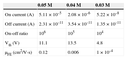
In Table 1, the mobility was observed to increase with solution concentration, with the highest value at 0.12cm2/V-s. The lowest μFE 1 × 10⁻⁴ cm2/V-s was found in TFTs with ZnO channel layer coating 0.02M solution. This result could be associated with mobility degradation caused by high grain-boundary density in the ZnO channel, as shown in AFM images (Fig. 3). As the grain size decreases, Vth increases. This occurs because, for a given channel dimension, the number of grain boundaries increases and the carriers will therefore have to overcome additional potential barriers. When the concentration of the ZnO solution is 0.05M, the on current is 5.11 × 10⁻⁵. At on state, the channel mobility is 0.12cm2/V-s, and the threshold voltage is 11.1V. Thus, the characteristic of TFT is the most stable for the ZnO solution concentration of 0.05M.
Electrical characteristics of the ZnO-TFT with different concentrations of ZnO solution.
| 0.05 M | 0.04 M | 0.03 M | |
|---|---|---|---|
| On current (A) | 5.11 × 10⁻⁵ | 2.08 × 10⁻⁶ | 5.22 × 10⁻⁸ |
| Off current (A) | 2.31 × 10⁻¹¹ | 3.54 × 10⁻¹¹ | 1.35 × 10⁻¹¹ |
| On-off ratio | 106 | 105 | 104 |
| Vth (V) | 11.1 | 13.5 | 4.8 |
| μFE (cm2/V-s) | 0.12 | 0.006 | 1 × 10⁻⁴ |
The drain current saturation characteristic for TFT operated in saturation regime is shown in Equation (1).
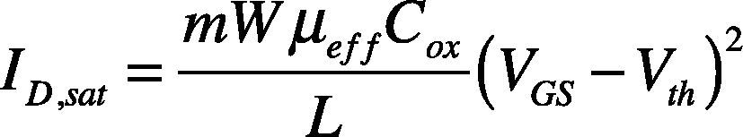
where m is doping density, W is channel width, L is channel width, COX is the gate oxide capacitance per unit area, and μeff is effective mobility. Threshold voltage is determined by plotting ID1/2 versus VG, and extrapolating the point of maximum slope (Anand et al., 2010).
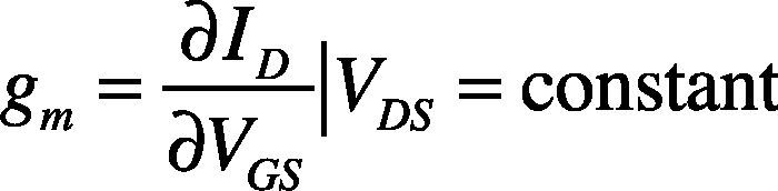
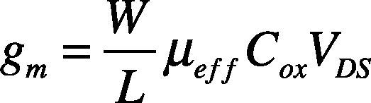
The field effect mobility (μFE) is determined from the transconductance (gm) expressed as:
When VGS>Vth, the drain current (ID) defined as
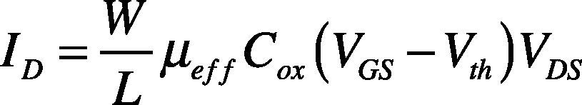
where W is channel width, L is channel length, COX is the gate oxide capacitance per unit area, and μeff is effective mobility.
The transconductance is usually expressed as
Thus, known as the field effect mobility
4Conclusions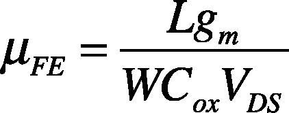
We investigated the structural, morphological, and electrical characteristics of ZnO films, coating various solution concentrations at room temperature, and monitoring their performance as active channels in TFT devices. We demonstrated that the characteristic of TFT is the most stable for the ZnO solution concentration of 0.05 M. When the concentration of the ZnO solution is 0.05M, the operation current level of a ZnO TFT is increased and the Ion/Ioff ratio is improved substantially. Under these conditions, the on-off current ratio is above 106, the channel mobility is 0.12cm2/V-s, and the threshold current is 11.4V. The average optical transmission of the ZnO film in the visible spectrum range is approximately 86%, and the transmission at 550 nm is 89%.
This work was supported by the National Science Council, Taiwan, under Contract Nos. MOST 103 – 2221 – E – 167 - 035.