


Thin films and coatings of permanent magnetic materials have found extensive applications in a wide range of technological domains. SmCo thin films show tremendous potential for use as permanent magnetic films on account of their high anisotropy fields, moderately high saturation magnetization and high curie temperature. In the present research, SmCo thin films have been deposited on single crystal Si(100) substrates using pulsed laser deposition technique. The films were deposited at a fixed substrate temperature of 400°C by varying the number of pulses, in order to get thin films of different thicknesses. Effect of laser pulses on the crystal structure evolution, composition of the deposited material, film thicknesses and hence the magnetic properties have been investigated. X-ray diffraction analysis was performed in order to determine the crystal structure of the deposited films. The compositional analysis was performed by using energy dispersive X-ray spectroscopy. A slight variation in the Sm and Co contents was observed in the thin films grown by varying the laser shots. The microstructural information of the thin films was obtained by using a scanning electron microscope. The magnetic and electrical parameters were investigated by using vibrating sample magnetometer and two point probe respectively. The results show hard magnetic and conducting nature of all deposited thin films except sample 1 due to poor crystallinity.
Since the discovery of SmCo5 as an excellent bulk material in the 1970s, a lot of effort has been invested to acquire better understanding of its magnetic properties and the optimal conditions of its fabrication. Nevertheless, there is a continuous quest to find optimum conditions for its defect-free fabrication in order to utilize them in the field of thin permanent magnetic films (Speliotis & Niarchos, 2005a). Pulsed laser deposition (PLD) is a relatively new technique that permits to grow thin films on a variety of substrates (Allocca, Gambardella, Morone, & Valentino, 2008). PLD-based thin films have been used in several applications, for instance, in electronics, high capacity memory supports, sensors, actuators and new spintronic-based valves. Recently, the possibility to growth thin magnetic film on insulator substrates like glass or commercial plastic, is of a great interest with the aim to fabricate low cost devices or components for many modern day applications (Allocca, Bonavolontà, Giardini, et al., 2008; Allocca, Bonavolontà, Lopizzo, et al., 2008). Owing to the excellent intrinsic magnetic properties, such as moderate saturation magnetization (Ms), large magnetic anisotropy and high Curie temperature (Tc), an extensive research has been devoted to investigate SmCo-based permanent magnetic thin films (Takei, Morisako, & Matsumoto, 2000). These films exhibit high coercivities (Hc) and remanences (Mr), adequate to create large fields in gaps in quasi-uniform magnetic circuits. In the field of reduced sized microelectromechanic systems (MEMS), these films become particularly relevant because they constitute the functional core of a broad range of MEMS which include, for instance, micromotors/microgenerators, sensors, polarizing devices and radio frequency micro switches (Neu, Thomas, Fähler, Holzapfel, & Schultz, 2002). In addition, SmCo-based permanent magnetic thin films are thermally stable enough to produce continuous magnetic fields with no energy consumption that can be employed for biasing the magnetic detectors for electronic industry, in particular (Andreescu & O'SHEA, 2001; Powers, Yan, Gao, Liou, & Sellmyer, 2002; Romero et al., 2007; Speliotis & Niarchos, 2005b). Hence, SmCo magnetic thin films have been considered as promising candidates for structured microelectromagnetic devices, when strong fields and high coercivities are involved (Allocca, Bonavolontà, Giardini, et al., 2008; Allocca, Bonavolontà, Lopizzo, et al., 2008; Yang, Han, You, & Zhang, 2003; Zangari, Lu, Laughlin, & Lambeth, 1999).
In the past, SmCo thin films have mainly been prepared by sputtering and, to our knowledge, no electrical properties on films prepared by pulsed laser deposition (PLD) in UHV have been reported (Romero et al., 2007; Zangari et al., 1999). SmCo films with hard magnetic properties have been prepared by pulsed laser deposition technique on different substrates by varying Sm content, but still the proper combination of good texture and high coercivity needs to be improved for good permanent magnet performance (Allocca, Bonavolontà, Giardini, et al., 2008; Allocca, Bonavolontà, Lopizzo, et al., 2008; Neu, Hannemann, Fähler, Holzapfel, & Schultz, 2002; Neu, Thomas, et al., 2002).
The present work focuses on the pulsed laser deposition of SmCo thin films on Si(100) substrate, by varying the laser shots in order to get thin films of varying thicknesses, and to subsequently investigate the structural, compositional and magnetic properties for utilizing these films as permanent magnetic data storage applications (Pina et al., 2005).
2Experimental proceduresThe deposition of SmCo thin films was carried out on Si(100) substrate by PLD technique. The frequency doubled Nd:YAG laser with wavelength of 532nm, pulse duration of 6ns, repetition rate of 10Hz and max pulse energy of 150mJ with circular beam size of 8mm was used as second source of irradiation. PLD chamber comprises of target station over which SmCo target is mounted with a facility to rotate and align the target with the laser beam. DC motor (24rev/min) was used to rotate the target with constant speed to ensure the uniform ablation. The substrate holder with resistive heater assembly parallel to target surface comprises of Si(100) wafer of size 15mm×15mm and thickness of 1mm. Optimized distance between target and substrate was set at 4.5cm. In the initial step, the sample was mounted on rotatable target holder inside the stainless steel chamber under ultra high vacuum (UHV) of 10−9torr. Argon gas was filled in the vacuum chamber at a pressure of 15mtorr for efficient momentum transfer. The temperature of Si substrate was 400°C and it was monitored by thermocouple (temperature sensor). The Nd:YAG laser of wavelength 532nm with energy density of 4J/cm2, spot size 2mm, pulse duration of 6ns and pulsed repetition rate of 10Hz was employed. It was focused onto SmCo surface through a lens of focal length 50cm. The beam hits the SmCo target at an angle of 45° as shown in Fig. 1. Five samples of SmCo thin films were deposited on Si(100) for various laser shots from 1000 to 5000, by ablating the SmCo5 target (Allocca, Bonavolontà, Giardini, et al., 2008; Allocca, Bonavolontà, Lopizzo, et al., 2008). The samples were characterized for its crystal structure using X-ray diffraction (XRD) technique. Electrical characterization of the thin film samples was carried out by a four-probe station. The surface morphology and compositional analysis was performed by a scanning electron microscope (SEM) and energy dispersive X-ray spectroscopy (EDX), respectively. Magnetic properties were determined by employing vibrating sample magnetometer (VSM).
3Results and discussion
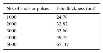
The X-ray diffraction analysis has been performed to investigate the crystal structure of deposited thin films. Fig. 2 shows the diffraction patterns of the thin films deposited on Si(100) substrate using 1000, 2000, 3000, 4000 and 5000 laser shots at a fixed substrate temperature of 400°C. The as-deposited SmCo thin films have already been reported to have amorphous behavior with a minute SmCo5 related peak with a (301) preferred orientation (You et al., 2007). In the present case, the deposited sample with 1000 laser shots mainly show amorphous behavior as no significant peak relating to the any phase of SmCo was evident. When the number of laser shots was increased to 3000, i.e., more thick film was deposited, a small peak at about 2θ=68.8° related to (301) plane of SmCo5 appeared, as seen in ICSD reference code 00-035-1400 and 00-027-1122 and as reported by Allocca, Bonavolontà, Giardini, et al. (2008) and Allocca, Bonavolontà, Lopizzo, et al. (2008). According to this reference, the deposited films have a hexagonal structure with space group P6/mmm, space group number 191. The corresponding lattice parameters were noted to be a=b=4.9970Å and c=3.9780Å. The intensity of this peak further increases as the laser shots increases from 4000 to 5000. The preferred orientation of the SmCo5 phase for the last three samples could be due to the high fluence laser shots. The preferred orientations of the present films were different from those of the films used in the previous work owing to the different processes and underlayer used (Hannachi, Belkacem, Bessais, & Mliki, 2016). In the present work, the preferred orientations were obtained after increasing laser shots. With increasing laser shots or film thickness SmCo5 peak becomes visible and stronger. Though the film thickness can affect the peak intensity, the much higher intensity of the (301) peak of the SmCo5 film with a thickness of 67nm implies an improved crystallinity. Thickness of the thin films was evaluated by spectroscopic ellipsometric method. Typical thicknesses of the deposited thin film samples in the series lie in the range of 25–67nm. Table 1 presented graphically in Fig. 3 According to the film thickness measurement results, it is obvious that the thickness increases by increasing the laser shots, which is understandable reason. As the laser shots increases more material is ablated from the target surface and subsequently deposited on the substrate surface. It is generally agreed that ablation becomes dominant with increasing the laser fluence and number of pulses. Therefore, deposition of ejected species on the substrate surface increases with increase in number of pulses. SmCo has non-linear absorption mechanism. It has weak absorption initially but subsequent laser pulses increase the absorption coefficient that would reduce the penetration depth and increase the heating at the surface.
 1000, (b) 2000, (c) 3000, (d) 4000, and (e) 5000 shots deposited by Nd: YAG Laser of wavelength 532nm at fixed substrate temperature of 400°C.")

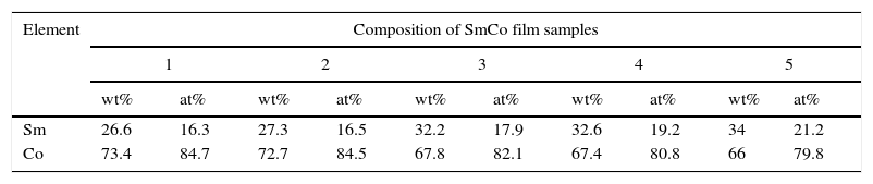
The chemical composition of different elements present in the thin film samples was determined by EDX analysis, in order to find the stoichiometric amounts of Sm and Co contents. Fig. 4 provides the SEM images and relevant EDX spectra of all the samples deposited by varying the number of laser shots from 1000 to 5000. The horizontal axis labeled in energy units and the vertical axis in intensity. The background in the given figures arises after several interactions of electron with the specimen while the other sharp and small spectral peaks are expected from the principles. In the EDX spectra, the sharp peak indicates the presence of silicon (contribution from the substrates, as Si(100) substrate is used in this work and small and wide peaks originate from the Sm and Co elements. The analysis also provides the information about percentage by weight (wt%) and atomic percent (at%) of each element present which shows that these samples contain a specific stoichiometric amounts of Sm and Co. Table 2 provides the variation in Sm and Co concentration in the samples deposited with 1000, 2000, 3000, 4000 and 5000 laser shots, and plotted graphically in Fig. 5. The plots reveal that as the number of laser shots is increased, the at% and wt% of Sm increase while those of Co decrease. From this trend, it is also evident that the composition of the third sample, which was deposited by using 3000 laser shots, keeping substrate temperature of 400°C, bears the closest composition to that of 1:5 phase of SmCo (Baig, Atiq, Bashir, Riaz, & Naseem, 2015).
 1000, (b) 2000, (c) 3000, (d) 4000, and (e) 5000.")

Fig. 3 reveals the SEM images of SmCo thin films on Si(100) substrate deposited by varying the laser shots. The micrographs mainly reveal a smooth, uniform and homogenous film surfaces. On most of the film surface, grain boundaries are not detected; however, some large sized grains deposited on the film surface can be seen. These grains might have been deposited during the post deposition environment ablated from the target surface as stray particles. The other reason for the presence of these grains might be attributed to the molten droplets and agglomerates of various shapes embedded on the surface of thin film that have been ejected from the molten pools of the target surface as a result of hydrodynamic sputtering and transported toward the substrate. The density of droplets depends upon the target morphology, laser spot size, fluence and background gas pressure (Chrisey & Hubler, 1994).
Fig. 6 shows the magnetic hysteresis (M-H) loops obtained at room temperature at an applied field of ±10kOe, in-plane to the sample surface. The values of Ms and Hc have been plotted for all the samples deposited by varying laser pulses. Mainly, all the deposited films show hard magnetic nature as the Hc values of all the SmCo films vary between 395.65 and 652.48Oe. These Hc values are quite sufficient to be exploited for magnetic recording and storage applications (Gerber, Wright, & Asti, 2013; Velu & Lambeth, 1992). It is obvious from the M-H loops that the applied field is not sufficient to fully saturate the deposited films. However the value of Ms obtained at an applied field of 10kOe varied between 124.76 and 140.38emu/cm3. The maximum value of Ms in this series of samples was evaluated for sample no. 3. From this, it is inferred that a deposition condition of 3000 laser pulses and a substrate temperature of 400°C are the optimum conditions to get avmaximum Ms value for the present series of samples.
 1000, (C) 2000, (D) 3000, (E) 4000, and (F) 5000.")
Fig. 7 shows the effect of laser shots (thickness) on the saturation magnetization and coercivity. The saturation magnetization increases by increasing the laser shots up to 3000 and then a sharp decrease in magnetization as we further increase laser shots. The coercivity also decreases by increasing the laser pulses up to 4000 and then increases. The increase in coercivity is due to high percentage of Sm content.

The electrical resistivity of the deposited films was calculated by two point probe technique. It was determined by measuring the ratio of the voltage drop (V) from the two probes to the applied current (I) measured from the same probes. The ratio V/I was multiplied by a geometric correction factor k=π/ln2 that depends up on the probe geometry. It has the value of 4.53 for a semi-infinite thin sheet. The film resistivity was calculated by using the relation as shown in Eq. (1). According to these results, the resistivity of the sample deposited at 1000 laser shots show maximum value of resistivity 0.317Ωcm. Afterwards, the value of resistivity decreases sharply and all the other four samples show values of resistivity varying between 0.02059 and 0.01774Ωcm, as drawn graphically in Fig. 7. The obvious reason for this change might be attributed to the amorphous behavior of the film deposited at 1000 laser shots. As the diffraction analysis reveals that the deposited thin films start to develop the crystalline texture of the SmCo5 phase at an increased number of laser shots, resulting in decreased resistivity and showing a more metallic behavior. However, all the samples show the conducting nature of the SmCo thin films except sample 1, due to its amorphous nature.
where ρ is the electrical resistivity (Ωcm), ‘V’ is the voltage measured in volts, ‘I’ is the source current in Amperes, ‘t’ is the thickness of the sample in cm (Benoy, Mohammed, Suresh Babu, Binu, & Pradeep, 2009).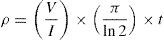
In Fig. 8 the graph shows that by increasing the laser shots, a sharp decrease in resistivity and an increase in conductivity have been observed. The initial decrease in resistivity and increase in conductivity attributable to a higher concentration of charge carriers due to improved crystallinity which makes the charge carriers more mobile. Further, an increase in the laser shots (thickness) increases the film conductivity. It is due to the formation of more ordered structures which contain the larger charge carriers and consequently mobility increases. In general, the thicker films have larger grains with lower density of grain boundaries, which behave as traps for free carriers and barriers for carrier transportation in the films. The thinner films with disordered structures exhibit a relatively small grain size and more boundaries. More stacking defects are generated in thinner films, which trap or scatter the carriers and retard the carrier mobility.
4Conclusions.")
In this work, SmCo thin films of various thickness have been deposited by varying laser shots and keeping the substrate temperature constant at 400°C, on Si(100) substrate using PLD. The diffraction analysis reveals the amorphous nature of the films deposited at 1000 and 2000 laser shots. However, when the films were deposited by increasing the number of pulses, a peak related to (301) plane of 1:5 phase of SmCo was evident. The scanning electron microscopy was employed to investigate the surface morphology and homogeneity of the deposited thin films. The micrographs reveal mainly a uniform surface with some large grains whose origin was attributed to molten droplets ejected because of hydrodynamic sputtering. The energy dispersive X-ray spectroscopy was utilized to determine the Sm and Co contents in at% and wt%. The M-H loops reveal that the sample deposited at substrate temperature of 400°C and 3000 laser pulses show a maximum value of saturation magnetization. The coercivity values of all the samples reveal hard magnetic nature of the SmCo thin films. The electrical properties show a conducting nature of all the samples except sample 1 which is due to an amorphous behavior.
Conflicts of interestThe authors have no conflicts of interest to declare.
The first author would like to thank Universiti Teknologi PETRONAS (UTP) for financial support (GA) Scheme and also the Center of Excellence in solid state physics and the Center for Advanced Studies in Physics for allowing to use their research facilities.
Peer Review under the responsibility of Universidad Nacional Autónoma de México.