


This work describes the optical and electrical characterization of an integrated optoelectronic receiver. The receiver is composed of a photodiode and a transimpedance amplifier, both fabricated in silicon technology using a 0.8μm BiCMOS process. The total area occupied by the photodiode is of 10,000μm2. In a first step, the generated photocurrent of the photodiode is measured for the wavelengths of 780nm and 830nm at different levels of optical power. In a second step, the responsivity and quantum efficiency parameters of the photodiode are computed. Finally, an electrical measurement including the transimpedance amplifier is achieved. A potential application for this optoelectronic receiver is on the first optical communications window.
Este artículo describe la caracterización óptica y eléctrica de un receptor optoelectrónico integrado. El receptor comprende un fotodiodo y un amplificador de transimpedancia, ambos fabricados en silicio utilizando tecnología de proceso BiCMOS de 0.8μm. El área total utilizada por el fotodiodo es de 10,000μm2. Inicialmente, se mide la fotocorriente generada por el fotodiodo para las longitudes de onda de 780nm y 830nm a diferentes niveles de potencia óptica. Posteriormente, se calculan los parámetros de responsividad y eficiencia cuántica del fotodiodo. Finalmente, se realiza una medición eléctrica que involucra al amplificador de transimpedancia. Una aplicación potencial para este receptor optoelectrónico se encuentra en la primera ventana de comunicaciones ópticas.
Currently, data transmission standards have an important role in optical communication systems. For this reason, an efficient design of the input stage is a critical issue for optoelectronic systems. An integrated input stage is composed of a superficial photodiode (PD) and a transimpedance amplifier (TIA) in a single chip, which is known as an optoelectronic integrated circuit (OEIC) [1]. The main characteristics required for an input stage are: high gain, extended bandwidth, low power consumption, minimum noise contributions and reduced area requirements. In this sense, optical and electrical devices fabricated in silicon technology allow satisfying the requirements previously cited [2–3]. The maturity of silicon technology represents a powerful platform that is truly compatible with standard CMOS processing [4–5], and by consequence, very attractive from the economic point of view. In this sense, the goal of this work resides in achieving a full performance evaluation of an integrated optoelectronic receiver that was designed by one of the authors [6]. This optoelectronic receiver is composed of a PD and a TIA fabricated in silicon technology in a 0.8μm BiCMOS process. The main advantage to use this technology resides in the fact that low-power supplies are used in relation to bipolar technology, solving in this way problems related to power consummation. In a first step, optical measurements are carried out, and then electrical measurements involving the amplifier are achieved.
Normally, photodetectors and transimpedance amplifiers are built in a separate way. In this work, we are presenting an electro-optical device that comprises both. An optical and electrical characterization was achieved guaranteeing in this way a complete performance. It is very important to remark that the measurements achieved are at a prototype level. The fabricated photodiode operates well at the wavelength of 830nm that corresponds to the first window optical communication, for this reason this electro-optical device has a potential application as a receptor module in an optical link. If well is truth that this wavelength is reserved only for short optical links, currently Local Area Network (LAN) operates at this wavelength allowing in this way a fast process of information.
2Receiver operating principleFigure 1 illustrates the basic scheme of an optical stage reception. The PD converts the incident optical power to an electrical current which is amplified by the TIA, obtaining in this way a corresponding voltage level (Vo) at its output. The feedback resistance (Rf) connected between the output and input of the TIA is used for amplification purposes.
2.1Photodiode operation
The PD was fabricated in a standard technology using a bulk process, and the diffused pn junctions are close to surface, as shown in Figure 2. An n-well region has been used to isolate the detector from substrate. The PD operates in avalanche mode to obtain an amplified signal and noise reduction. Since the p++ is used as collect layer, the pn junction is close to the surface and the photodiode area can be easily illuminated by using a multimode or monomode optical fiber.

The equivalent circuit corresponding to a PD is illustrated in Figure 3, where Ip is the generated photocurrent, Id is the dark current, Cs is the junction capacitance, Rs, Rsh, and RL, are the series, sheet and load resistance, respectively.

Since Xcs≪Rsh at high frequencies and assuming that Rs is less than 100Ω because it represents the contact resistance, which was reduced by layout techniques and the resistance of the undepleted silicon, model of Figure 3 can be simplified to the equivalent circuit shown in figure 4. RL was substituted for the input impedance of the TIA.

The responsivity parameter of the PD can be computed as [7]
where Po is the incident optical power, η is the quantum efficiency, q is the electron charge, hv is photon energy, and the quantum efficiency can be evaluated by3Transimpedance amplifier operation

The CMOS TIA structure used in this work is based on the common-gate topology, using negative feedback. Because a negative feedback is used at the input transistor, the bandwidth is increased and the noise contributions are reduced. The TIA amplifier diagram is shown in Figure 5.

The transfer function achieved by using a local feedback network is in Equation (3)
where is is the photogenerated current including Ip and Id, gm1 and gm2 are transconductances of transistors M1 and M2, respectively. The cgd2 and cgs2 are the gate-drain and gain-source capacitances of the transistor M2, respectively. The cgs1 is the gain-source capacitance of the transistor M1. The cp1 and cs are the output load and photodiode capacitances, respectively, and finally the gf1 is the load resistance of the TIA amplifier. The TIA gain is given by Rf when s → 0. A transimpedance gain of 40dB and a bandwidth of 2GHz were obtained using an Rf of 100Ω and a output capacitance of 0.3pF. A further description of the design of the TIA is given in [6].4Description of the optoelectronic integrated circuit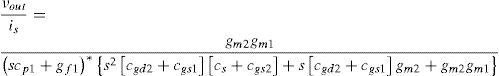
This integrated optoelectronic receiver monolithically integrates a PD and a preamplifier circuit. Process BiCMOS AMS technology is used for this purpose using minimum dimensions of 0.8μm. Figure 6 shows a photograph of the integrated optical stage receptor in which the PD and the TIA are indicated.

As was previously mentioned, this manufacturing process allows the pn junction to be very near the surface allowing the PD area to be illuminated independently of the TIA. Figure 7 corresponds to a zoom of the last photograph corresponding only to the PD. Its dimensions are 100μm×100μm.

The chip containing the optoelectronic integrated circuit is glued on a FR4 substrate, and the pads are welded to the lines of a printed circuit in order to allow its connection to the electrical equipment. Figure 8 corresponds to a picture of this prototype.

Figure 9 shows a zoom of the optoelectronic integrated circuit where detail of the interconnection between pads and connection lines is clearly observable.
4.1Measuring of the photocurrent
Electrical and optical characterization is an important step because provides information that allows corroborates the good performance of the device. In this sense, in the following a complete optical and electrical characterization is described. For this goal we have used an Electro/Optical Converter (Gravizon model LL-780GI, λ=780nm), and a modulable laser unit (Lasiris, λ=830nm). A visible sensor head (Thorlabs, model S120A) is attached to an optical power meter system (Thorlabs, model S110), in order to verify the wavelength and measure the optical power of the devices previously mentioned. Optical powers of P=640μW and P=40mW are measured for the Electro/Optical Converter and the modulable laser unit, respectively. Figure 10 corresponds to the experimental setup used to measure the photocurrent of the photodiode. The light issued from the laser is coupled to a segment of standard multimode optical fiber (62.5μm/0.27) and attached to a test point in order to guide the light as near as possible to the PD area. An external amperimeter (Keithley multimeter, model 2001) closes the circuit under measure in order to record the values of current. A variable DC source (+V) allows a DC sweep in the range of 0 to –18V.

In a first step, the PD is polarized in reverse-bias in order to measure the reverse leakage photocurrent (or dark current) produced without illumination. Figure 11 corresponds to the measured current level whose range is in nanoampers, and the breakdown voltage is located around −17V.

In a second step, the PD is illuminated by using the electro/optical converter Gravizon. Its corresponding results are illustrated in Figure 12. In this case, the photocurrent value is increased because of the illumination and is in the order of microampers.

Finally, the PD is now illuminated by using the modulable laser unit. Figure 13 plots the measured photocurrent. In this case and because of the high incident optical power, the values of current in the order of milliamps is remarkable.
4.2Evaluation of the quantum efficiency
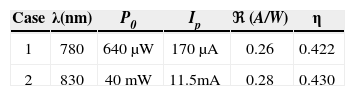
Once the levels of photocurrent are known, for simplicity, the photons reflected at the face of the photodiode are omitted. The responsivity and quantum efficiency are determined from Equation (1) and (2), respectively. Table 1 shows these results.
The low value corresponding to the responsivity parameter is justified by the absence of an antireflectance film at the face of the photodiode.
5Transimpedance amplifier stageAs was previously mentioned, the integrated optoelectronic receiver monolithically integrates a PD and a preamplifier circuit, which is shown in Figure 14, which illustrates the experimental setup used to test the optoelectronic stage including the amplifier. In this case, the amplifier is operated as follower voltage. The electro/optical converter is modulated by a sinusoidal signal by using a signal generator (Rhode … Schwarz, Model SM101).

The input of the amplifier is short-circuited to its output in order to operate as follower voltage. The modulated light issue of the E/O converter is coupled again to a segment of standard multimode optical fiber in order to illuminate the area of the photodiode. The polarization voltage (Vcc) applied to the photodiode is fixed to -3 volts. Channel 1 of an oscilloscope (Tektronix, TDS3054B) allows monitoring the sinusoidal signal (f=1.589MHz and Vpp=1.14V) applied to the E/O converter, whereas channel 2 permits recovering the output signal. Upper and lower traces illustrated in Figure 15 correspond to the screen of the oscilloscope showing the applied and recovered signal, respectively. A good result without a noticeable degradation is clearly observable.

Figure 16 shows a comparison between the simulated and experimental result of the frequency response of the optical system. In the experimental test, measurements were made using a Wiltron vector-analyzer model 360 and a Tektronix S-parameters test model 576. A bandwidth of 1.9GHz and 0.8GHz was obtained by simulated and experimental ways, respectively.
6Conclusions
A full optical and electrical characterization of an integrated optoelectronic receiver was achieved. It is well known that a factor that affects the number of photon incidents, and thus the quantum efficiency, is the absence of an anti-reflection coating on the surface of the photodiode; hence, the values computed for this device are within an acceptable range. It is true that the quantum efficiency could be increased by increasing the thickness of the intrinsic region to allow more absorption of photons, but the price would be to increase the response time of the device. On the other hand, the moderate frequency response of the device is justified by the technique used to illuminate the photodiode and the interconnection lines to the FR4 substrate. However, this can be improved if the optical fiber is launched directly over the photodiode area. It is clear that the optical wavelengths used for this characterization correspond to the first optical window communications; therefore, this integrated optoelectronic receiver is found to have a potential and practical application in this window.