


In this work, the synthesis and the structural, morphological and electrical characterization of Ce1−xSmxO2−δ solid solution, with x=0, 0.10, 0.15, 0.20, 0.25 and 0.30mol, are reported. Nanocrystalline, homogeneous, and adherent samarium doped cerium oxide thin films were deposited onto glass (Pyrex®) substrates by a simple and cost effective ultrasonic spray pyrolysis system, at a low substrate temperature of 450°C and further annealing treatment at 500°C for 2h. For all the samples, X-ray diffraction results showed the formation of single phase and well crystalline thin films, with cubic fluorite type structure. Scanning electron microscopy analyses showed homogeneous surfaces for all the samples; from SEM micrographs crystallite sizes were found to be in the range 23–37nm. From atomic force microscopy, surface roughness in the range of 20–95nm was measured and the formation of smooth films with an average grain size of 45nm was observed. For the best sample in the solid solution, high oxygen ion conductivity of 1.71×10⁻¹Scm−1, at 450°C, was determined by impedance spectroscopy, with an activation energy of 0.93eV. Results suggest that these films may have a potential application as electrolytes in intermediate temperature solid oxide fuel cells, IT-SOFC.
En este trabajo se reporta la síntesis y caracterización estructural, morfológica y eléctrica de la solución sólida Ce1−xSmxO2−δ, con x=0, 0,10, 0,15, 0,20, 0,25 y 0,30mol. Se depositaron películas delgadas de óxido de cerio dopado con samario nanoestructuradas, homogéneas y con buena adherencia sobre sustratos de vidrio (Pyrex®) mediante un sistema de rocío pirolítico ultrasónico sencillo y económico, a una baja temperatura de 450°C y con un tratamiento térmico adicional a 500°C por 2h. Para todas las muestras, los resultados obtenidos por difracción de rayos X mostraron la presencia de películas delgadas cristalinas monofásicas, con estructura cúbica tipo fluorita. Los análisis de microscopía electrónica de barrido mostraron superficies homogéneas para todas las muestras; a partir de las micrografías SEM se determinó que los tamaños de los cristales se encontraban en el intervalo de 23-37nm. A partir de microscopía de fuerza atómica se midió la rugosidad superficial en el rango de 20 a 95nm y se observó la formación de películas homogéneas con un tamaño promedio de grano de 45nm. Para la mejor muestra, mediante espectroscopia de impedancias se determinó una alta conductividad de iones de oxígeno de 1,71×10⁻¹Scm−1, a 450°C, con una energía de activación de 0,93eV. Los resultados sugieren que estas películas pueden tener una potencial aplicación como electrolitos en celdas de combustible de óxidos sólidos de temperatura intermedia, IT-SOFC.
In recent years, solid oxide fuel cells (SOFC) have been of interest to the scientific community due to their ability to promote clean, green and high efficiency energy conversion [1–5]. However, the high operating temperature, around 1000°C, makes the selection of materials very limited. On the other hand, two of the main research goals for SOFC are the efficiency improvement and the reduction of the operation temperature of these devices, by an appropriate selection of materials [6–8]. Efficiency is mainly related to the improvement of electrolyte materials, which must have high ionic conductivity, high chemical stability, high density and must to be thin materials. Among those materials that can be used as solid electrolytes, because of their important advantages like long-term stability and economical competitiveness [9], ceria-based materials have been widely studied as the alternative for yttrium stabilized zirconia (YSZ) commonly used as electrolyte in SOFC. Furthermore, samarium doped cerium (SDC) thin films may reduce not only the resistance but also the operation temperature of SOFC [10–15].
Several techniques have been used to prepare thin film electrolytes, such as screen printing [16], tape casting [17], pulse laser deposition [18], cathodic sputtering [19], electron deposition (EB-PVD) [12], and spray pyrolysis [20–26]. Among these methods, spray pyrolysis is a simple, low cost and integrated process to produce large area and well adherence films with controlled morphology and uniform thickness.
Spray pyrolysis consists of three consecutive steps, after atomization of a liquid precursor containing metal salts into droplets, they travel toward a heated substrate and film formation occurs and, finally, the evaporation of the solvent and decomposition of the deposited material takes place [27–30].
This technique, under ambient pressure, provides high flexibility in terms of the materials composition, it is an appropriate method for the deposition of a wide variety of thin films since the addition of dopants to the spray solution is simple it is easy to prepare films of any composition by simply mixing the components in the appropriate ratios [20].
In this research, dense and homogeneous nanocrystalline Ce1−xSmxO2−δ thin films, with x=0, 0.10, 0.15, 0.20, 0.25 and 0.30mol, were successfully deposited by ultrasonic spray pyrolysis technique, at low substrate temperature of 450°C. The structural, morphological and transport properties of annealed films, at 500°C for 2h, are reported.
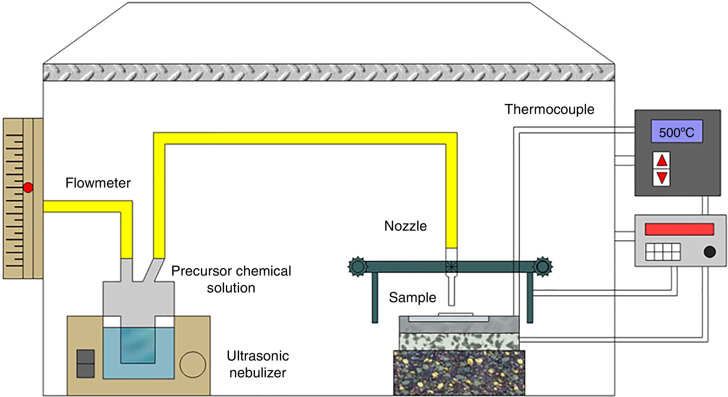
Experimental procedureThin films preparationA typical ultrasonic spray pyrolysis (USP) system is shown in Fig. 1. The nebulizer delivers ultrasonic waves generated by the high frequency vibration (1.7MHz) of a piezoelectric transducer in order to atomize the precursor chemical solution into a stream of fine droplets, 1–5μm.

Cerium (III) acetylacetonate hydrate Ce(C5H7O2)3·xH2O (Sigma Aldrich, 99.9%) and Samarium (III) acetylacetonate hydrate C15H21SmO6·xH2O (Sigma Aldrich, 99.9%) in appropriate amounts, and dissolved in 0.036M dimethylformamide HCON (CH3)2 (J. T. Baker, 99.93%), were used as reactive precursors.
To obtain Ce1−xSmxO2−δ thin films, after precursor chemical solutions were prepared they were carried under an air flow of 120mL/min and a scanning speed of 0.005m/s to the substrates, which were kept at 1cm from the nozzle. Films were deposited onto glass substrates (2cm×2cm) previously ultrasonically cleaned, in ethanol, for 10min. Deposited films were allowed to cool slowly and then placed in a desiccator.
In the ultrasonic spray pyrolysis method, the substrate temperature plays an important role for phase formation and crystallinity of the films. To obtain the optimal value, substrate temperature was varied in the range 350–450°C with an interval of 50°C. In order to study the effect of annealing temperature on phase formation and crystallinity of the products, films, which were deposited under above mentioned substrate temperature, were annealed at 450°C and 500°C, for 2h each.
Structural and morphological characterizationX-ray diffraction (XRD) is a powerful technique not only to identify the crystalline structure of materials but also to analyze several structural properties such as phase composition, grain size, preferred orientation, strain, and defect structure. Thin films were analyzed by XRD technique using a Siemens D500 diffractometer, with CuKα1 radiation, λ=1. 54056Å. The operation conditions of the diffractometer were 34kV and 25mA to produce an intense X-ray beam whose incidence angle was 1°. Step size and time/step were 0.02° and 1.2s, respectively. Measurements were performed from 20 to 70 2θ degrees. Phases in all compounds were identified using EVA software and ICDD data base (JCPDS cards). OriginLab software was employed for measuring the Full Width at Half Maximum (FWHM) of the most intense peaks to calculate the crystallite size (d) by using the Scherrer equation
where λ is the X-ray wavelength, β is the FWHM of the peaks and θ is the diffraction angle.
Morphological characterization of thin films was performed with a field emission scanning electron microscopy (SEM) JEOL JSM 7600F, equipped with X-ray energy detector X_ACT Oxford INCA for chemical analyses. Working conditions included a low accelerating voltage from 1 to 5kV, and work distances in the range 4–10mm. The obtained images were acquired with secondary electrons.
In order to complete the morphological characterization, atomic force microscopy (AFM) technique was carried out. Analyses were performed with a microscope JEOL JSPM-4210. Images were obtained in tapping mode and results were analyzed using the WinSPM DPD software version 2.0.
Transport propertiesTransport properties of thin films were performed by impedance spectroscopy technique. Impedance measurements of films were carried out in air between 150 and 500°C in the frequency range from 0.1Hz to 10MHz, using a Solartron 1260 Impedance Analyzer attached with a 1296 Dielectric Interface. Two small parallel areas, which were used as electrodes, were made on the surface of thin films with carbon paste (PELCO high temperature carbon paste, Ted Pella, Inc.). Conductivities of thin films were determined using the Z-View software, from Nyquist plots results were modeled as parallel equivalent circuits connected in series.
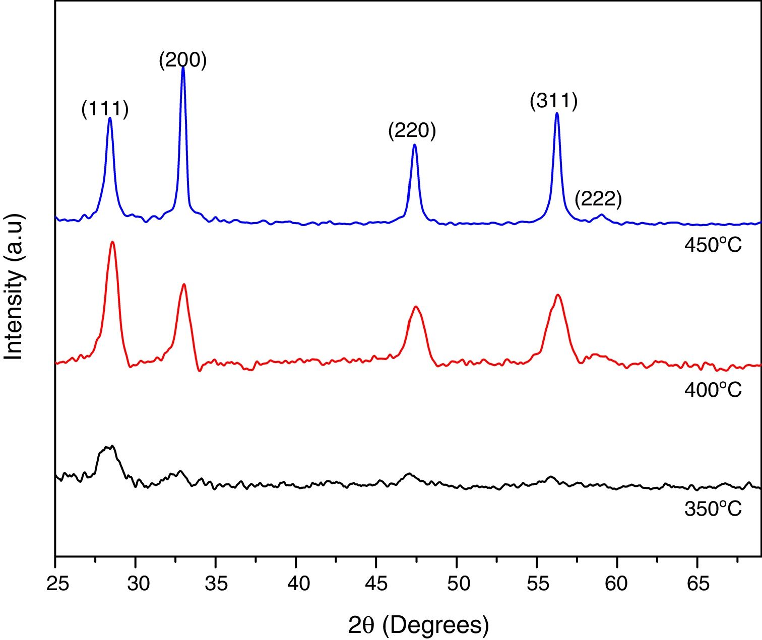
Results and discussionStructural analysisTo obtain high quality Ce1−xSmxO2−δ compounds, the substrate temperature for the deposition of thin films was varied in the range 350–450°C, with steps of 50°C, and the kinetic growth was analyzed by XRD to identify the best substrate and annealing temperatures. For 350°C, compounds showed a partial amorphous nature probably because the decomposition of the precursor solutions have not been completed, however the substrate temperature strongly affects the growth of (111) and (200) peaks, when temperature reaches 400°C the preferred orientation changes to (200) plane. When the substrate temperature increases, the films become more crystallite, as indicated by the increased intensity of the (200) peak however the corresponding FWHM decreased, Fig. 2. From these results, optimized substrate temperature for the deposition of Ce1−xSmxO2−δ thin films was found to be 450°C, also the crystallinity was enhanced with a further thermal treatment at 500°C for 2h. From now these conditions, 450°C for synthesis and 500°C for annealing temperatures will be taken for all Ce1−xSmxO2−δ thin films.

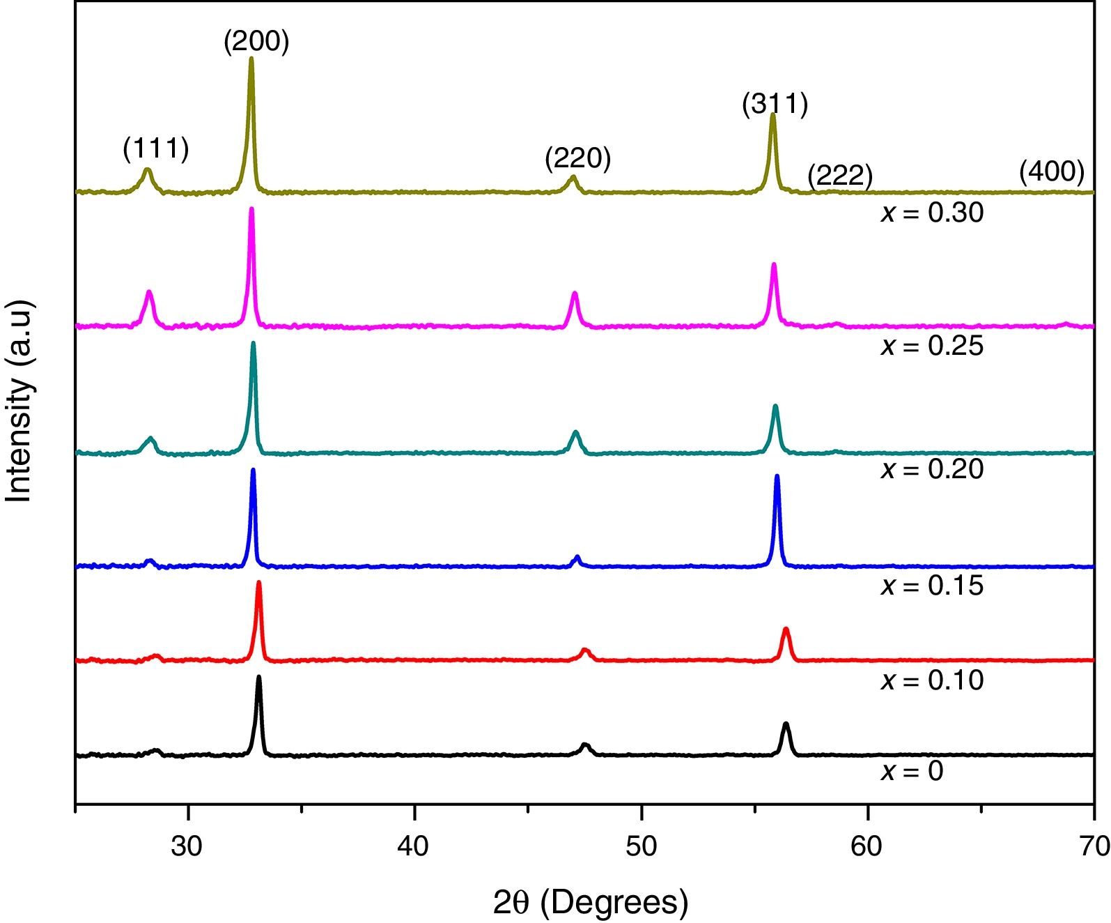
XRD patterns of samarium doped ceria thin films are shown in Fig. 3. It was found that all compositions are well crystallized single phase products with a cubic fluorite type crystal structure, (ICDD file 04-013-4361), which corresponds to a space group Fm-3m (225). For all compositions, wide peaks in the XRD patterns indicate nanocrystalline products. Also, from XRD results it can be observed that under the deposition conditions, all the samples exhibit preferential orientation along the (200) plane [15,31–33].

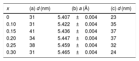
The average size of crystallites was calculated by using the Scherrer formula, Eq. (1), to the (111), (200), and (220) diffraction peaks. For all compositions, peak shapes were fitted to a pseudo Voigt function profile. For the most intense peaks, (200), average grain sizes are shown in Table 1a.
For Ce1−xSmxO2−δ thin films: (a) average grain size, d, calculated from Scherrer's equation. (b) Lattice parameters, a, obtained with CELREF software. (c) Average grain size, d, obtained from SEM images.
| x | (a) d (nm) | (b) a (Å) | (c) d (nm) |
|---|---|---|---|
| 0 | 31 | 5.407±0.004 | 23 |
| 0.10 | 31 | 5.422±0.004 | 35 |
| 0.15 | 41 | 5.436±0.004 | 37 |
| 0.20 | 34 | 5.447±0.004 | 37 |
| 0.25 | 38 | 5.459±0.004 | 32 |
| 0.30 | 31 | 5.465±0.004 | 24 |
Indexing of diffraction patterns was performed using DICVOL [34,35] software with WinplotR/Fullprof package, the cell type and the lattice parameters were determined by the least squares method (CELREF software) [36]. After obtaining the cell parameters a refinement of these values were carried out to minimize the dispersion between experimental and calculated values. Table 1b shows the lattice parameters of Ce1−xSmxO2−δ, thin films.
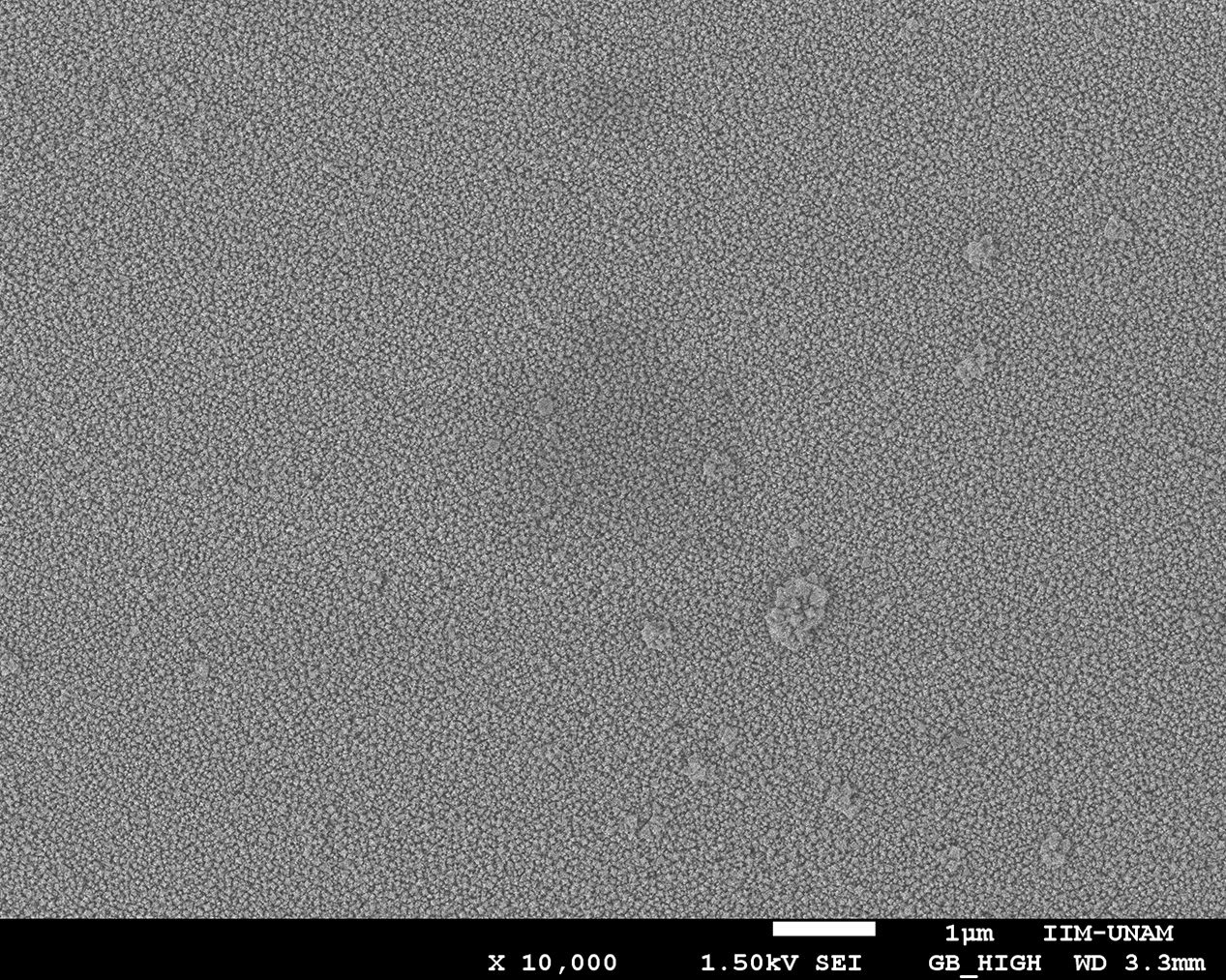
Morphological resultsSEM micrograph of Ce0.8Sm0.2O2−δ thin film, which was synthesized at 400°C without further heating treatment is shown in Fig. 4. This image shows a surface morphology free of cracks with small agglomerates probably because the decomposition of the precursor solution has not been completed.

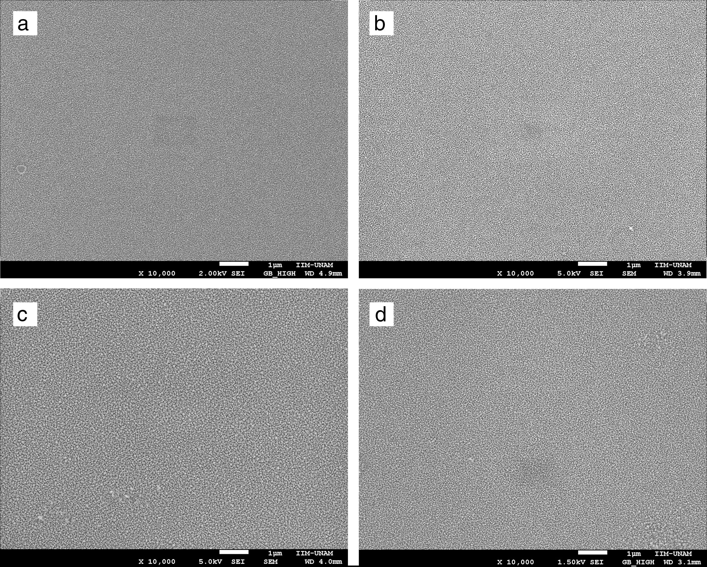
SEM micrographs of Ce1−xSmxO2−δ thin films prepared at 450°C and sintered at 500°C for 2h show no cracks, Fig. 5(a)–(d). Uniform surfaces composed of fine grains are clearly observed, which indicate a complete decomposition and evaporation of precursor deposited on the substrates. Screen Caliper software, version 4.0, was used to measure the grain sizes observed in SEM micrographs; results are shown in Table 1c.
 at 10000× magnification: (a) x=0, (b) x=0.15, (c) x=0.20, and (d) x=0.30.")
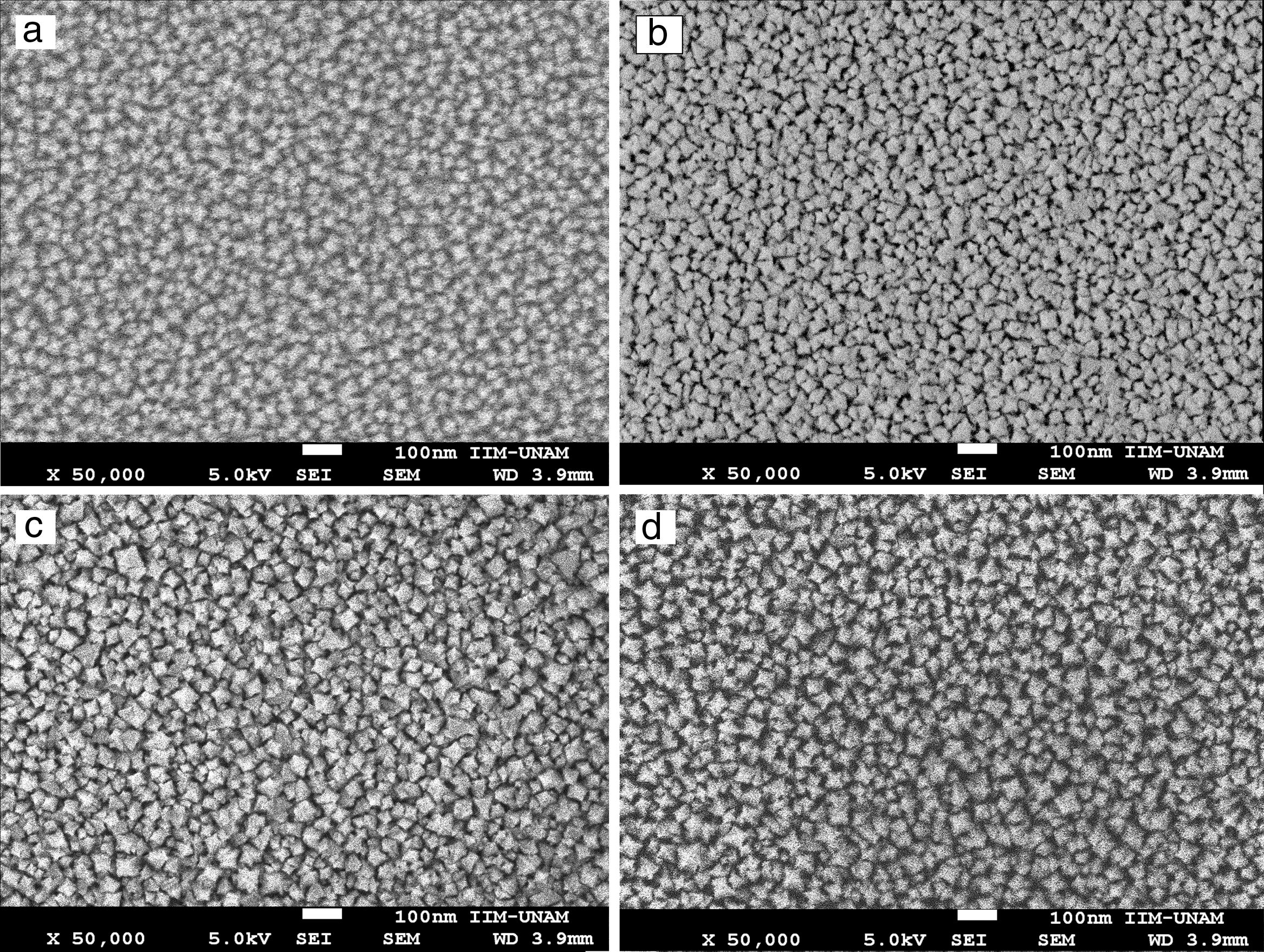
High magnification SEM images revealed that Ce1−xSmxO2−δ compounds consist of nanostructured particles around 30nm in size. This size calculation is rather consistent with the crystallites size determined by XRD using the Scherrer's equation, i.e. the broad peaks appeared in the XRD patterns are due to the presence of nanosized Ce1−xSmxO2−δ crystallites in the films. For all compounds, micrographs show a rough morphology with popcorn shaped clusters, it seems that the addition of samarium promotes a grain growth with triangular shape. At higher magnification, 50000×, grains of Ce0.85Sm0.15O2−δ and Ce0.80Sm0.20O2−δ are slightly larger than those of the other compositions, Fig. 6.
 at 50000× magnification: (a) x=0, (b) x=0.15, (c) x=0.20, and (d) x=0.30.")
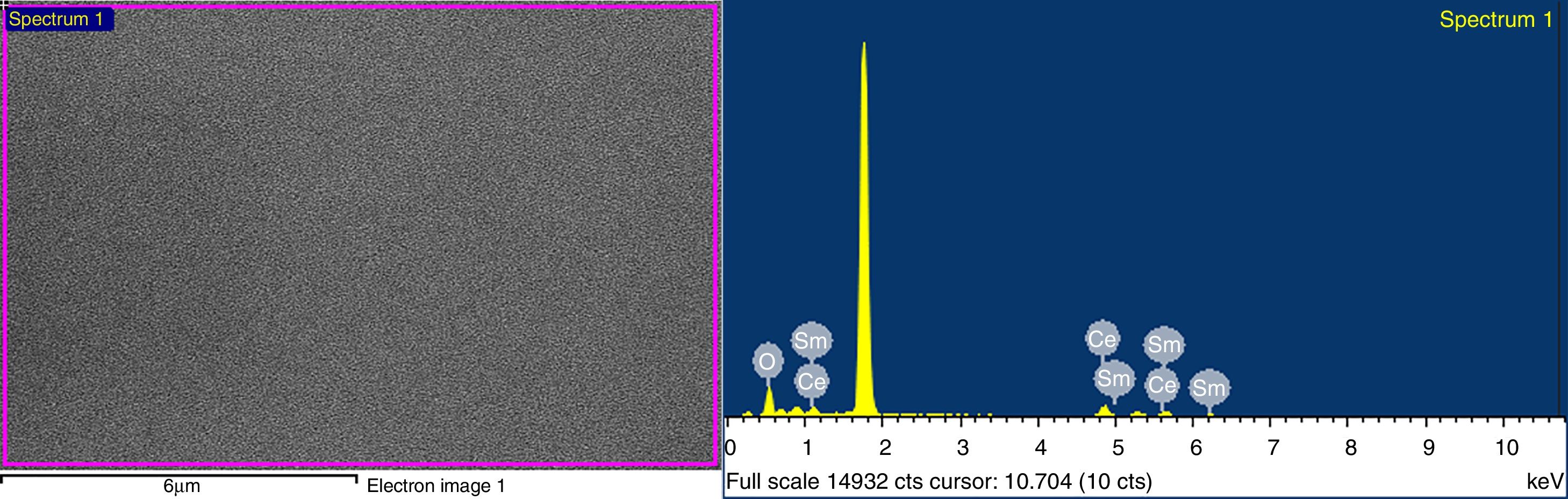
EDX spectra of Ce1−xSmxO2−δ thin films were carried out; for x>0 results confirmed the presence of Ce, Sm and O in all films. The EDX spectrum of Ce1−xSmxO2−δ, for x=0.2, synthesized at 450°C and annealed at 500°C is shown in Fig. 7.
 from the glass substrate.")
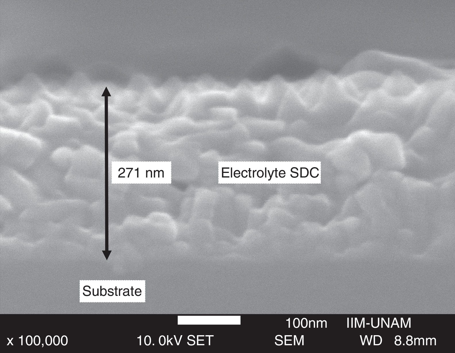
Cross-section micrographs were obtained to determine the thickness of deposited thin films, measured values are in the range 100–350nm; images also showed dense films with adequate adhesion to the substrate. The cross-section micrograph of Ce0.80Sm0.20O2−δ thin film is shown in Fig. 8.

Additional morphological studies by AFM were carried out. For all samples, the surface roughness and grain sizes of the products were determined. Values for grain sizes were obtained using WinSPM DPS software V2.0, and the average roughness of thin films by the formula
f(x, y) it is the height of the peaks in the analysis plane, Z0 is the average height of the peaks in terms of analysis and S0 is the plane area analysis.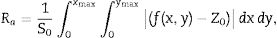
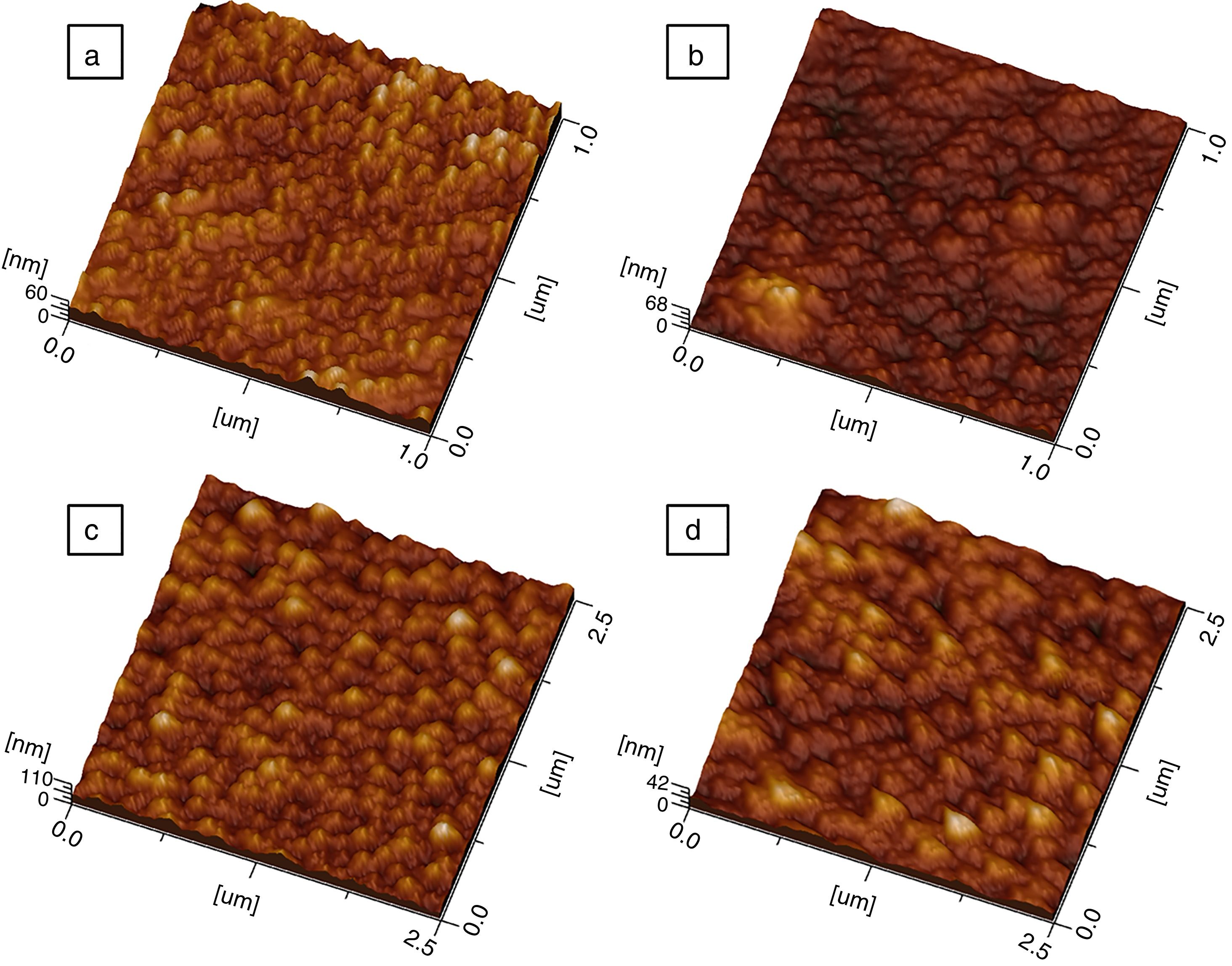
Fig. 9 shows three-dimensional AFM images of the thin films surface topography. In Fig. 9(a) and (c), which belongs to CeO2 and Ce0.85Sm0.15O2−δ respectively, high surface homogeneity can be observed. For these films, the surface morphology is composed of small granules with almost spherical shape, which average sizes are 80 and 95nm. Fig. 9(b) and (d) shows images of Ce0.80Sm0.20O2−δ and Ce0.70Sm0.30O2−δ, respectively; regular surfaces are also observed but now the average sizes of the agglomerates, 190 and 210nm, are larger compared to those observed for x=0 and x=0.15. Average roughness (Ra) was calculated from Eq. (2) for all the films, these values are in the range of 20–95nm. In this work, the surface morphology shows the formation process of the thin films by using the USP method. After the atomized particles are dispersed toward the surface of the glass, the temperature of the substrate is such that the finest droplets are likely to react chemically before reaching the substrate and they are grouped one on top of the other until they crystallize, however the homogeneity is adversely affected producing the profile and roughness (Ra) observed on the surface of the films [37], these morphological results are similar to those previously reported by Sriubas and Kwak [12,38].
: (a) x=0, (b) x=0.15, (c) x=0.20, and (d) x=0.30.")
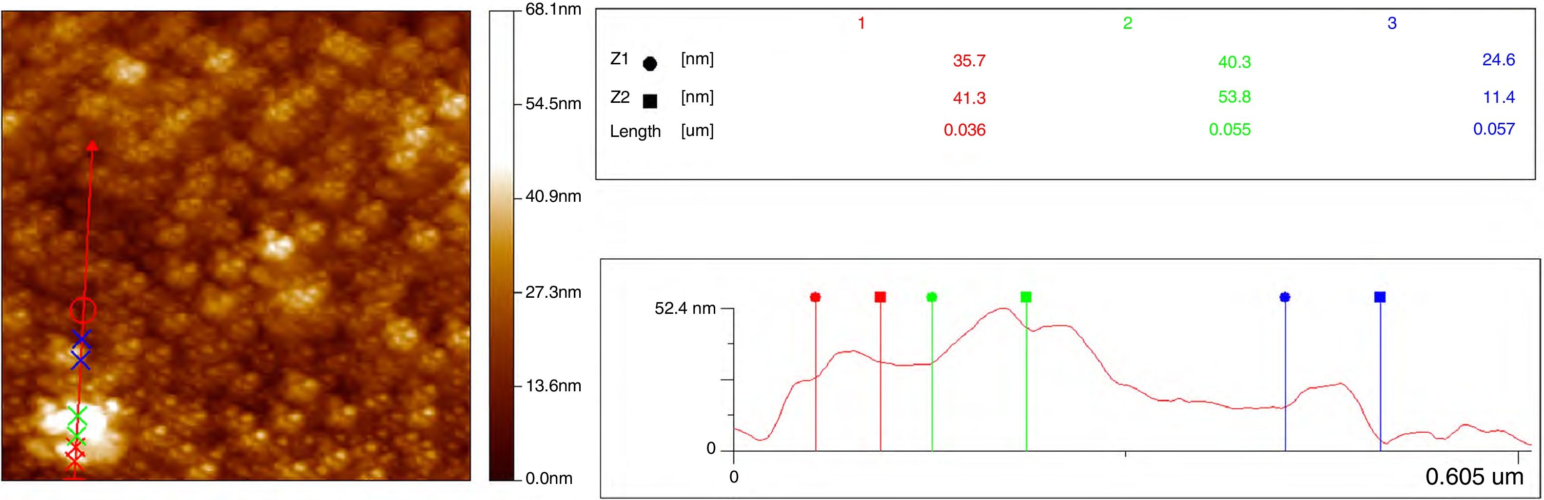
Two-dimensional AFM images were used to determine the grain sizes of all compounds, measurements indicated that these values are in the range 30–60nm and agreed those values obtained from SEM micrographs. Fig. 10 shows the AFM profile of Ce0.80Sm0.20O2−δ.
Transport properties
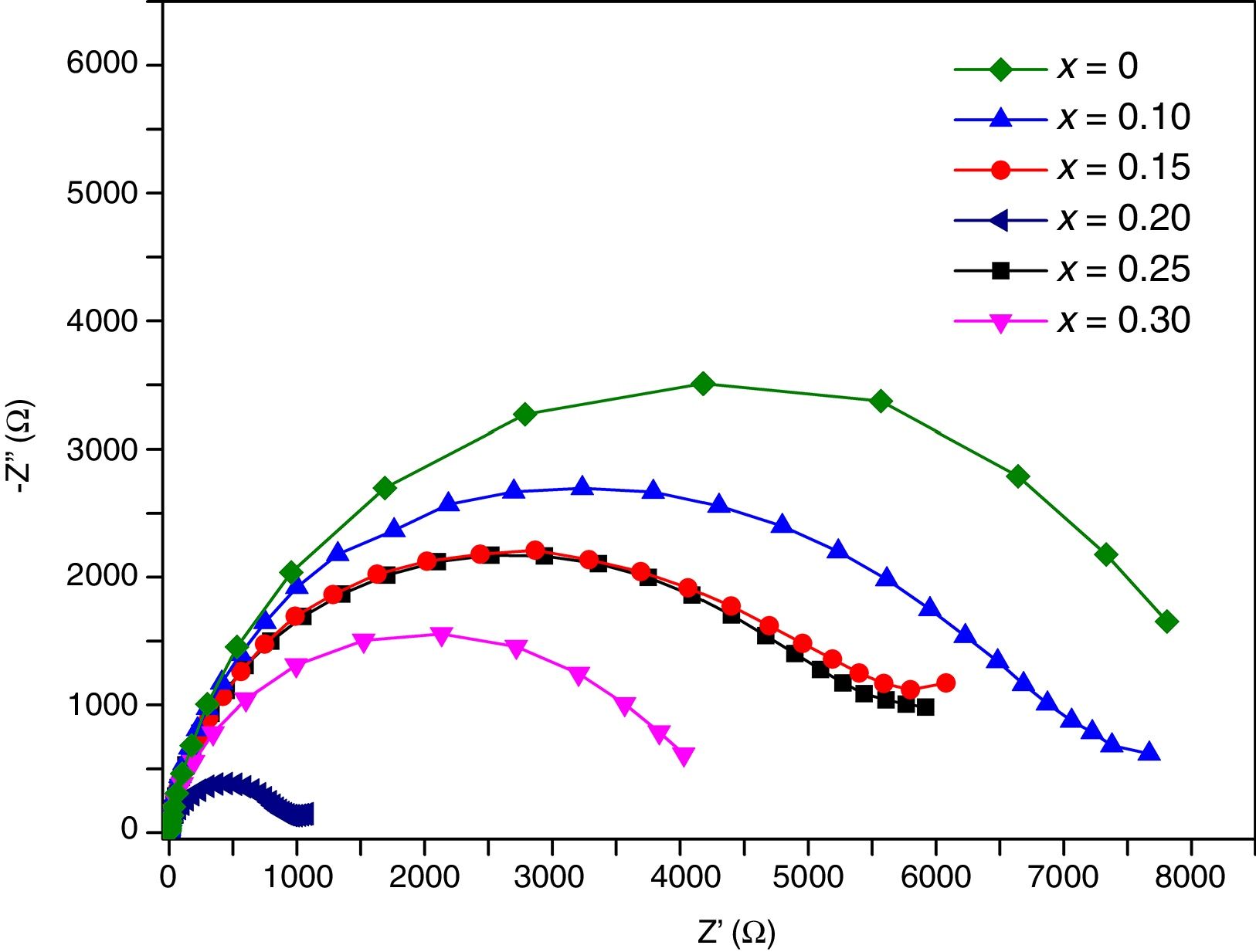
Impedance measurements of thin films were performed in air, in the temperature range 200°C–500°C. Typical complex impedance plots (Z′ vs –Z″), at 400°C, are shown in Fig. 11. These Nyquist graphs showed only one incomplete arc, which corresponds to grain resistance (Rb). Above 300°C these arcs are well-resolved, however at higher temperatures bulk resistances gradually decrease and approximately at 500°C the arcs disappeared. The contribution of the bulk was clearly identified from its high frequency response and characteristic capacitance, calculated of the pF order of magnitude.

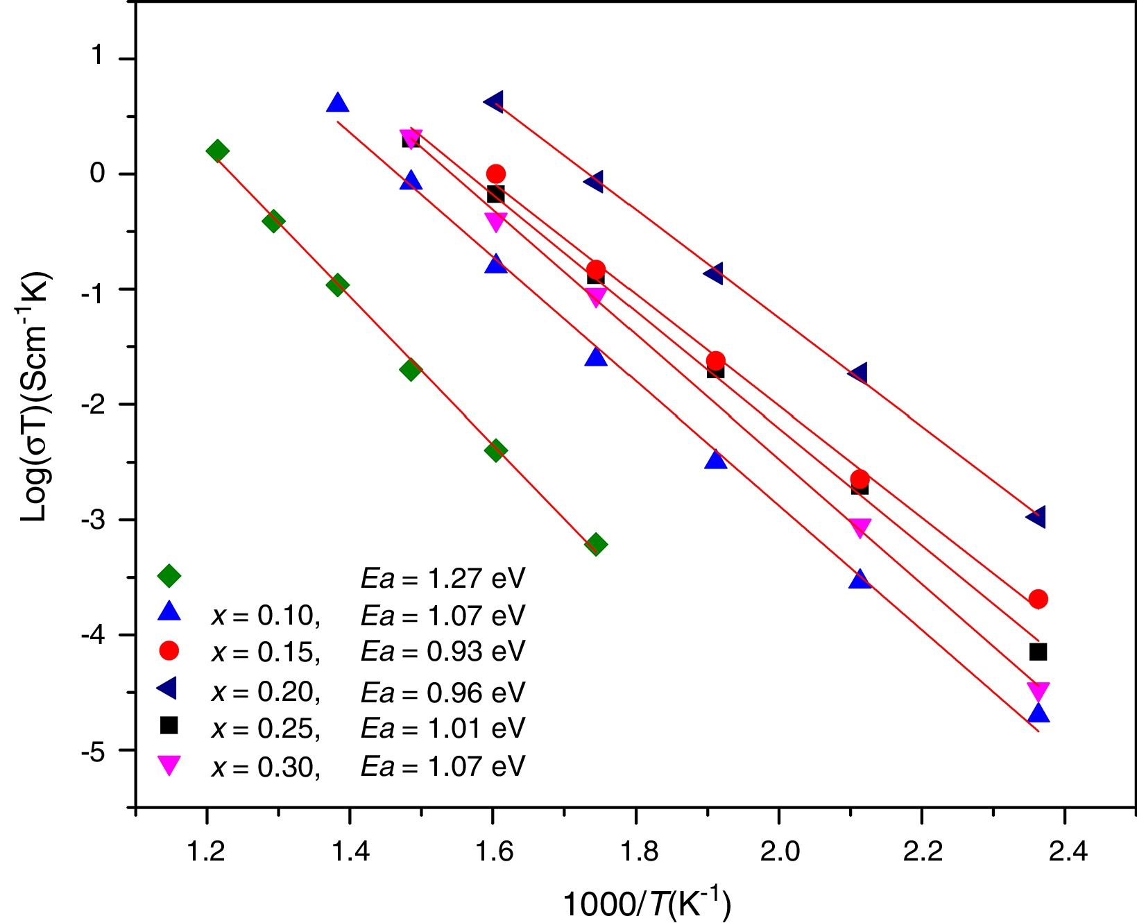
Conductivity data were used to calculate the activation energy of thin films with the Arrhenius equation
where Ea is the activation energy for conduction (eV), T is the absolute temperature (Kelvin), k Boltzmann's constant and σ0 is a pre-exponential factor. In this work, electrode resistances were not considered for the total conductivity calculations. From the logσT vs 1000/T plots, linear adjustments by least squares were carried out to obtain the activation energies, Fig. 12; these values are in the range reported by Sriubas and Li [13,39] and also even lower than those reported by Virbukas [14].

Although the best conductivity was observed for the sample Ce0.80Sm0.20O2−δ, results showed that the activation energy was minimum for the composition Ce0.85Sm0.15O2−δ. The difference in activation energies of Ce1−xSmxO2−δ, in the range of 0.93 to 1.27eV, may be attributed to an order-disorder transition of the oxygen sublattice. This decrease is due to the presence of attractive interactions between dopant cations and oxygen vacancies. In fact, it has been mentioned that the activation energy of oxygen vacancy concentration may depend on the dopant since a high concentration of dopants can generate doping grouping and associated oxygen vacancies, which may reduce their mobility. An increase in the RE dopant content for the Ce1−xSmxO2−δ solid solution prevents oxygen-ordering leading to an increase in activation energy and decrease in ionic conductivity in ceria. Thus, the maximum ionic conductivity and the minimum activation energy are not always associated with the same concentration of dopant [40–43].
Impedance responses were modeled by equivalent circuits using the Zview 3.3 program. The equivalent circuit that fitted the impedance data consisted of a resistor, Rb, and a constant phase element, CPE, connected in parallel. Due to depression of arcs, the use of a simple capacitor was not sufficient to model the electrical response of thin films, thus a CPE was used to fit these results [44].
ConclusionsThe ultrasonic spray pyrolysis technique was satisfactory to deposit nanocrystalline Ce1−xSmxO2−δ thin films on glass substrates by simple and low cost ultrasonic spray pyrolysis technique. Uniform and dense films were synthesized at temperatures as low as 450°C, and based on the behavior of the most intense peak, (200), well crystallized compounds were obtained with a further annealing at 500°C. For all compounds, XRD results showed single phase products with cubic fluorite type structure with space group Fm-3m; it was possible to determine the lattice parameters, and a slight shift to higher angles was observed with composition, i.e. at higher concentration of the dopant the lattice parameter of the compound increased systematically. The average crystalline size calculated by the Scherrer equation was 35nm. The SEM morphological characterization of thin films depicted uniform homogeneous and crack-free surfaces with pop-corn like structure for all compositions with grain sizes between 23 and 37nm. For all the films, AFM results showed homogeneous surfaces composed of agglomerates with average sizes in the range 90–210nm. The transport properties of thin films, which were analyzed by impedance spectroscopy, indicated that the conductivity of these compounds, from 1.71×10⁻¹ to 4.43×10⁻⁴Scm−1 at 450°C, was dominated by grains, with activation energies in the range 0.93–1.27eV. Results suggest that these films, in particular those with x=0.15 and 0.20, may be used as solid electrolytes in intermediate temperature solid oxide fuel cells (IT-SOFC).
RMB (366093) thanks CONACyT for the 245587 scholarship. Authors acknowledge the technical assistance of O. Novelo-Peralta, C. Flores-Morales and M. Garcia-Hipolito (IIM-UNAM), and also PAPIIT–IN119010 (DGAPA-UNAM) and ECOS 229381 (ANUIES-CONACYT) projects for financial support.