


Polycrystalline thin film solar cells made with absorber materials such as CdTe, CIGS, CZTS and metalorganic halides (perovskites) are currently important alternatives for the silicon solar cell technology, which still dominates the photovoltaic market. Then, it is important to have tools which can be used to design this kind of solar cells. For this purpose, we have developed a unified simple analytical model that can be applied to thin film solar cells. The model is based on the basic physics of hetero-junction devices, but it takes into consideration that the space charge region can extend along the major part of the cell length, particularly for very thin cells, causing important effects that typically are not observed in conventional junction devices. Photo-generated carriers are collected by electric field-drift instead of diffusion, and simultaneously strong recombination at this region may dominate the electrical I–V characteristic of the cell. Since the space-charge region width varies with the applied voltage, the illumination current density and the saturation dark current density are no longer independent of the voltage as is assumed for conventional solar cells. When the model is applied to CIS and CdTe solar cells as examples, it is found that it is possible to design very thin film solar cells (absorber less than 1μm thick) with high efficiencies, whenever the recombination velocity at the back surface becomes small (102cm/s), instead of the high recombination velocities present at ohmic contacts (107cm/s). This fact implies the cost reduction of thin film solar cells by reducing absorber material thickness, and therefore it poses a challenge to develop deposition methods for very thin CdTe and CIGS absorber materials without pinholes, so that improved efficiencies are obtained when the surface recombination velocity is made small at the back by having a p+ or an electron blocking region before the ohmic contact. This result also explains the high efficiencies achieved by very thin perovskite solar cells.
There is the expectation that thin film solar cells will be the alternative to silicon solar cells which is the dominant technology at the photovoltaic market today. Improved efficiencies and lower costs of thin film solar cells are required for this goal to become a reality. Among the most developed thin film solar cells we have CdS/CdTe and CdS/CIGS which recently have attained efficiencies above 20% (Green, Emery, Hishikawa, Warta, & Dunlop, 2015). Each one of these technologies needs solving some problems related to the quality of the deposited materials (by different techniques), but as it will be shown here, reducing the film thickness and achieving higher open circuit voltages are required for both kind of solar cells. However, in general, CdTe and CIS solar cells are studied independently of each other without having a more integral vision.
It must be observed that from the structural point of view, CdTe and CIS solar cells are similar and therefore their physical behavior is also identical. The change is in the absorbing material (with their own properties) and the technological steps followed to make the solar cells. For example, CdTe is typically obtained by closed space vapor transport (CSVT) or Rf-sputtering (Morales-Acevedo, 2006), while CIS solar cells are obtained by co-evaporation or Rf-sputtering among other different techniques (Singh & Patra, 2010). CdTe typically cannot be p-type doped above 1015cm−3, and cells with small CdTe thickness cannot be easily done because pinholes cause the device degradation. Then, present CdTe minimum thickness is around 4–6μm. In the case of CIS solar cells, the CIS (or CIGS) thickness is around 3–4μm.
It will be shown that good cells can be designed with absorber thickness around 1μm or below. Hence, the technological challenge is achieving CdTe and CIS materials with good properties, but without pinholes using the present or new deposition techniques. In such a case, the amount of material would be reduced by about 60–75% with a corresponding decrease in the total cost of the cells.
In this paper, we shall describe a simple analytical model that can be used for the above mentioned solar cells (CdTe and CIS), so that they can be designed easily. This model is complete in the sense that it includes carrier transport limited by diffusion and by generation–recombination at the space charge region. It also takes into account that the space charge region width is dependent upon the operating voltage and therefore the superposition principle is no longer valid. In other words, the current density due to illumination is not a constant with respect to the applied voltage, but it has some dependence upon this variable. Similarly, the total dark saturation current density will not be independent of the operating voltage, as it is usually assumed.
Having a simple model that considers the above effects for thin film solar cells is very important because, in general, they are not taken into account because for conventional cells, such as those made with silicon, these effects are negligible. Conventional junction silicon solar cells are typically made with absorber thickness of more than 200μm, so that the space charge region effects on good solar cells are small because the depletion region thickness is of the order of 1μm.
For thin film solar cells, the space region effects become important because the total volumes of the space charge region and the quasi-neutral regions are of the same order, particularly for very thin film solar cells. Furthermore, under some situations (which depends upon the equilibrium majority carrier concentration and the thickness of the absorbing material) the depletion region may extend along the whole length of the absorbing material. In this case, the recombination in the depletion region will limit the total dark current, but at the same time the photo-generated carriers will be collected efficiently because of the presence of the high electric field in this region. And this electric field will be larger for thinner solar cells. Hence, there is a complex relation between majority carrier concentration (Na), absorbing thickness, lifetime and mobility of minority carriers for the whole operating voltage range of the solar cell. The main objective for this work will be to have a simple model that takes into consideration all the above effects.
It will be shown that the model predicts that if the recombination at the back surface is reduced, for example by having a p+ region before the back contact, so that surface recombination velocities are small (102cm/s or less) compared to the high recombination velocities obtained at ohmic contacts (above 107cm/s), then very thin cells can achieve improved efficiencies than those with thick absorbers because of the reduction of bulk recombination, although there might be some loss of photo-current density.
Finally, in order to have a complete model for designing thin film solar cells, the optical design was also considered by using the optical matrix method applied to all the films that are part of the cells. The electrical and optical calculations were applied to CdTe and CIS solar cells, as an example of the application of the models described here.
2I–V modelingThe reference structure of a thin film solar cell is shown in Figure 1. It is formed by three main regions: The transparent conducting oxide (TCO) which allows the light passing to the hetero-junction, the window semiconductor layer (typically CdS), and the absorbing semiconductor material. Ohmic contacts are both made at the back of the absorbing layer and at the front TCO layer in order to connect the cell to the external circuit. We shall assume that the back is covered by a metallic contact which reflects totally those photons that pass the absorbing layer without being absorbed causing a second pass of such photons through this layer.

As explained above, an important parameter that determines the electric and photoelectric properties in a solar cell is the thickness of the space charge region (depletion region) in both the p-type and n-type sides of the heterojunction by means of the following expressions:
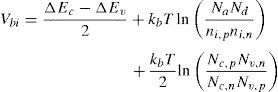
where ¿p is the relative permittivity of the p-type material and ¿n is that of the n-type one, Na and Nd are the acceptor and donor concentrations at each region, respectively, V is the bias voltage and Vbi is the built-in potential, calculated as:where ΔEc and ΔEv are the conduction and valence band discontinuities, respectively. kb is the Boltzmann constant, ni,p and ni,n are the intrinsic carrier concentrations of the p and n-type materials. Nc,p and Nc,n are the effective densities of states in the conduction band of the p and n-type materials and finally Nv,p and Nv,n are the effective densities of states in the valence band of the p and n-type materials.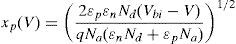
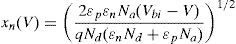
In some cases, xp as calculated by Eq. (1) might be larger than the thickness of the absorber layer itself (Wp). In this case, the depletion region would extend over the entire material, so that the depletion region would be limited by the thickness of the absorber layer (i.e., xp=Wp and xn=Wp(Na/Nd)). This condition could be changed as the forward operating voltage is increased because the depletion thickness is reduced as the forward voltage is increased.
To determine the total photocurrent density, there are two contributions to be considered. The one limited by carrier diffusion and the one due to the electric field drift of the generated carriers at the space charge region. For each wavelength λ, it is necessary to consider the transmittance T(λ) in the TCO layer, and the total reflectance R(λ) due to the multilayer system, as will be determined in the next section.
The photocurrent density limited by ambipolar diffusion at the quasi-neutral regions are given by Kosyachenko (2010) and Nelson (2003):
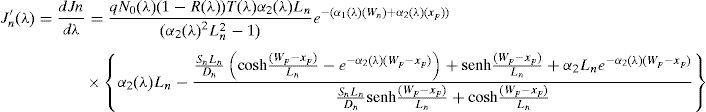
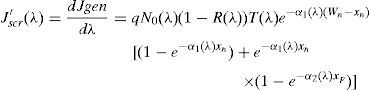
In addition, the photocurrent density due to the carriers generated (a 100% collection efficiency is assumed under the influence of the high electric field) at the space charge region will be:Ln and Lp are the minority carrier diffusion lengths, Wp and Wn are the p and n layer thickness, respectively, and Sp and Sn are the respective surface recombination velocities. In all cases, the photon density flux N0(λ) corresponds to the AM1.5G standard solar spectrum. The absorption coefficients of the window layer α1(λ) and the absorber layer α2(λ) were considered in the same wavelength range up to the wavelength that can be absorbed by a specific absorber material. Photons with larger wavelengths will not produce any photo-current.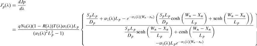
The total current density is the sum of each of the above current densities (J′p, J′n and J′scr) and integrated in the range between λmin (300nm) and λmax (850nm for CdTe and 1200nm for CIS, which correspond to the absorption edges of the CdTe and CIS layers, respectively). It is given by the following expression:
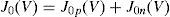
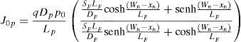
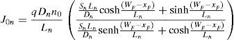
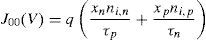
The dark current components will also be limited either by diffusion or by generation–recombination at the space-charge region (Sze, 2008).where T is the temperature, k is the Boltzmann constant, and J0 and J00 are the dark saturation currents due to diffusion and generation–recombination, respectively. They are given bywhereandni,n and ni,p are the intrinsic carrier densities, p0 and n0 are the minority carrier concentrations, and τp and τn are the minority carrier lifetimes, in the n and p semiconductors, respectively.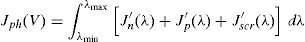
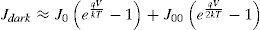
Therefore, all the dark saturation current density components depend upon the operating voltage because xp and xn are functions of this variable, as given by Eqs. (1) and (2). The total current density of the cell is then given by:
From this J–V dependence the maximum generated power can be determined by assuming the series and shunt resistance losses to be zero. The efficiency will be given bywhere Jm and Vm are the current density and voltage at the maximum power point, respectively, and Pinc is the incident radiation power density.

Notice that the above model uses well known expressions, but they unified into a simple full analytical model for including the effects mentioned in the preceding section. Including these effects is important for quantifying in a more complete manner the behavior of thin film solar cells.
3Optical modelA simple way to evaluate the optical losses for a thin film solar cell is to use the optical matrix method. The optical matrix is expressed in terms of Fresnel coefficients for a system of m layers, where the mth and (m−1)th are layers with complex refractive index nm=nm−ikm and nm−1=nm−1−ikm−1.
The optical matrix for the mth layer is defined by the following expression (Heavens, 1954):
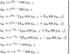
where each of the elements are calculated in accordance to the following set of equations:gm and hm are functions that depend on both the refractive index and the extinction coefficient. The values of α and γ can be calculated accordingly towhere λ is the wavelength and d is the respective layer thickness. The reflectance R(λ) for a system of four layers on a substrate is calculated aswhere t1,4, u1,4, p1,4 and q1,4 are the equivalent elements of the product of the optical matrices for each layer.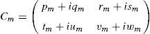
Based on this model, as well as on the values of refractive index n(λ) and extinction coefficient k(λ) reported in the literature (see Fig. 2) (Filmetrics, 2016; Mclntosh, 2016; Pan, Zhang, Teng, Li, & Li, 2008; Polyanskiy, 2016; Treharne et al., 2011), values of R(λ) were determined for the solar cells studied in this paper, as will be discussed in the next section.
4Application of the model to CIS solar cells The refractive index and (b) the extinction coefficient for ZnO:Al, Mo, CIS, CdS, SnO2 and CdTe films.")
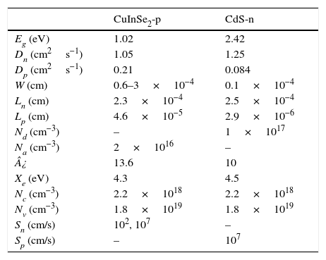
With the purpose of determining the efficiency of a CIS solar cell, schematically shown in Figure 3, the relevant physical parameters were obtained from previous reports (Table 1). The value of the CIS absorber layer thickness was varied between 500nm and 3000nm in order to obtain the solar cell efficiency. The band diagram of the structure under equilibrium was built by applying Anderson's rule (Fig. 4) (Anderson, 1960; Sharma & Purohit, 1974), in which the bandgap values and characteristic electron affinities are observed.

Values for the parameters used in the calculations of CIS solar cell (Amin, Tang, & Sopian, 2007; Benmira & Aida, 2013; Busacca et al., 2014; Daza et al., 2017; Kasap & Capper, 2006; Slonopas et al., 2016; Touafek, Aida, & Mahamdi, 2012).
| CuInSe2-p | CdS-n | |
|---|---|---|
| Eg (eV) | 1.02 | 2.42 |
| Dn (cm2s−1) | 1.05 | 1.25 |
| Dp (cm2s−1) | 0.21 | 0.084 |
| W (cm) | 0.6–3×10⁻⁴ | 0.1×10⁻⁴ |
| Ln (cm) | 2.3×10⁻⁴ | 2.5×10⁻⁴ |
| Lp (cm) | 4.6×10⁻⁵ | 2.9×10⁻⁶ |
| Nd (cm−3) | – | 1×10¹⁷ |
| Na (cm−3) | 2×10¹⁶ | – |
| ¿ | 13.6 | 10 |
| Xe (eV) | 4.3 | 4.5 |
| Nc (cm−3) | 2.2×10¹⁸ | 2.2×10¹⁸ |
| Nv (cm−3) | 1.8×10¹⁹ | 1.8×10¹⁹ |
| Sn (cm/s) | 102, 107 | – |
| Sp (cm/s) | – | 107 |

In Figure 5, the result of R(λ) for the ZnO:Al/CdS/CIS/Mo/glass structure in the 300–1200nm region (CIS absorption edge) is observed. In the graph, a characteristic behavior with oscillations due to interference effects at different wavelengths is evident. This behavior is expected because of the thickness and refractive index difference of the AZO material compared to that of CdS and the other layers below (Mahdjoub & Hadjeris, 2013).

A complete calculation of the solar cell efficiency is made taking into account the transmittance as a function of wavelength T(λ) for the above cell structure. In this case, a transmittance average around 80% (above the ZnO:Al absorption edge) is obtained, which is in good agreement with other reported theoretical and experimental results (Bernal-Correa, Morales-Acevedo, Montes-Monsalve, & Pulzara-Mora, 2016; Kuwahata & Minemoto, 2014).
Based on the values shown in Table 1, as well as the results for R(λ), T(λ), and taking into account the spectra for α1(λ) and α2(λ), Jph was calculated using the model described in Section 2. The photons not absorbed in the first pass of light through the cell structure are reflected at the back contact, so that these photons must be included for the calculation of the light current density because they have a second opportunity to be absorbed by the absorber layer. This additional photo-current has also been calculated, although it is not given explicitly in the expressions for Jph, above.
The values of Jsc as a function of the CIS thickness are shown in Figure 6. For a high recombination velocity at the back (107cm/s), a rapid decrease of the Jsc (mA/cm2) is observed for absorber layer thicknesses lower than 3μm, in accordance with the behavior reported in the published literature for CIS solar cells (Ibdah et al., 2014; Matin-Bhuiyan, Shafkat-Islam, & Jyoti-Datta, 2012; Tivanov, Astashenok, Fedotov, & Węgierek, 2012). However, for a low back recombination velocity (102cm/s), there is an optimum thickness below 1000nm.

Figure 7 shows the results of internal quantum efficiency IQE(λ) and external quantum efficiency EQE(λ) as functions of the photon wavelength for a CIS solar cell with absorber layer thickness of 3000nm and high recombination velocity at the back (107cm/s). In Figure 7, we can see clearly that the difference between IQE and EQE is due to the optical effects associated to the optical transmittance and reflectance for the given solar cell structure (shown in Fig. 5). Particularly for wavelengths below 450nm, the EQE is greatly reduced as a consequence of the reduced transmittance at the front layer. The J–V and P–V characteristic curves were also calculated, from which Jm, Vm and Voc, FF and efficiency (η) were determined, as shown in Figure 8.


Results for solar cell efficiency when varying thickness of the absorber layer are shown in Figure 9. Notice that when the surface recombination velocity is low at the back, the optimum CIS thickness is small (around 750nm), which is in agreement to what was explained in Section 1. Then, the material required can be reduced with the respective reduction of cost, and at the same time a high cell efficiency can be expected. Hence, it is convenient to have the reduction of the surface recombination velocity at the back, while achieving high quality absorber thin films without pinholes. These are objectives to be pursued in future CIS or CIGS and CdTe solar cells, as well.
5Efficiency of a CdS/CdTe solar cell
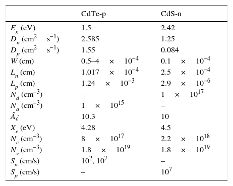
The developed model was also applied to determine the expected efficiency for CdS/CdTe solar cells, like the one illustrated in Figure 10 with the band diagram shown in Figure 11. The physical parameters used in the simulations are displayed in Table 2. In this case, the CdTe absorber layer thickness was varied between 500nm and 4000nm. Thickness for the CdS layer was the same as for the CIS cell (100nm). In addition, the thickness of the SnO2 layer was assumed to be 500nm (similar to the ZnO:Al layer thickness in the CIS cell).


Parameters used in the calculations of the CdS/CdTe solar cell (Amin, Sopian, & Konagai, 2007; Amin, Tang, et al., 2007; Benmira & Aida, 2013; Busacca et al., 2014; Daza et al., 2017; Fardi & Buny, 2013; Kasap & Capper, 2006; Khosroabadi, Keshmiri, & Marjani, 2014; Slonopas et al., 2016; Touafek et al., 2012).
| CdTe-p | CdS-n | |
|---|---|---|
| Eg (eV) | 1.5 | 2.42 |
| Dn (cm2s−1) | 2.585 | 1.25 |
| Dp (cm2s−1) | 1.55 | 0.084 |
| W (cm) | 0.5–4×10⁻⁴ | 0.1×10⁻⁴ |
| Ln (cm) | 1.017×10⁻⁴ | 2.5×10⁻⁴ |
| Lp (cm) | 1.24×10⁻³ | 2.9×10⁻⁶ |
| Nd (cm−3) | – | 1×10¹⁷ |
| Na (cm−3) | 1×10¹⁵ | – |
| ¿ | 10.3 | 10 |
| Xe (eV) | 4.28 | 4.5 |
| Nc (cm−3) | 8×10¹⁷ | 2.2×10¹⁸ |
| Nv (cm−3) | 1.8×10¹⁹ | 1.8×10¹⁹ |
| Sn (cm/s) | 102, 107 | – |
| Sp (cm/s) | – | 107 |
The calculated reflectance R(λ) and transmittance T(λ) of the structure depicted in Figure 10 is shown in Figure 12 in the range of 300–850nm. The range of wavelength is shorter than for the CIS cell since the absorption edge of CdTe is smaller than for CIS films. It is worth mentioning that the average reflectance in this structure is smaller than for the above CIS structure (less than 6%).

Table 2 contains the physical parameters for CdS and CdTe used in the calculation of the solar cell mentioned above. The calculation was also made for two values of back recombination velocity Sn. The low recombination velocity value can be achieved by having a specially treated CdTe layer. For example, an etching at the back may cause a tellurium rich surface, achieving a p+ region. In addition, Morales-Acevedo (2014) has suggested the inclusion of an additional back p+ layer of another material, such as ZnTe, forming a back heterojunction that blocks electrons flowing to the back contact. This minority carrier blocking should reduce strongly the recombination velocity at the back.
The short-circuit current density results are shown in Figure 13. It can be observed that its highest value is obtained at low recombination velocities; nevertheless, it does not correspond to the thinnest CdTe layer, but to an intermediate value. This can be explained by acknowledging that in a very thin layer the depletion region (and the associated electrostatic field) can extend over its entirety but it absorbs less light than a thick one; on the other hand, in a very thick layer the incident light is practically absorbed in its totality, but the depletion region extends only over a narrow part of the material and hence the electron-hole pairs photo-generated outside this depletion region have a lower probability to be collected, which in turn is reflected in a decrease of the short-circuit current.

Figure 14 shows the external and internal quantum efficiency for the CdS/CdTe solar cell with a CdTe thickness of 1μm and back recombination velocity of 102cm/s, which corresponds to the cell with the best performance as will be seen in Figure 16.

In Figure 15, the expected J–V and P–V curves (current density and power as functions of voltage) of the solar cell with a CdTe thickness of 1μm and back recombination velocity of 102cm/s are presented. J–V and P–V curves of solar cells with different thicknesses were also calculated, nevertheless this was the solar cell with the highest efficiency.

Figure 16(a)–(c) shows the output parameters of the solar cell as functions of the CdTe thickness. From a quick glance at these graphs, the Voc and FF have their highest values at 0.5μm and they decrease as the CdTe layer becomes thicker for Sn=102cm/s; this behavior has been explained in Section 1 and seems to be in good agreement with other works (Morales-Acevedo, 2014) and it is due to the reduction of the surface recombination velocity at the back contact. The highest value obtained for Voc is 947mV and for the fill factor, 0.847 when the CdTe thickness is around 500nm. Regarding the efficiency, the highest value obtained is 18.66% and it is once again achieved with a low back recombination velocity (Sn=102cm/s) and with a CdTe thickness of 1μm.

As a general observation, the best results are achieved with a low back surface recombination velocity and small thickness. It is also important to notice that for thick CdTe layers, the recombination velocity does not have a significant effect on the outcome of the cell parameters.
Notice that reported record efficiencies for CdTe solar cells are above those calculated here, but the results shown here correspond to the expected efficiencies when the transport parameters are those given in Table 2. These parameters are typical for most of the reported cells in different laboratories around the world. Record efficiencies above 20% might correspond to an absorber layer which is not pure CdTe, as can be observed from quantum efficiency measurements made on record cells (Green et al., 2015), and possibly the material has been prepared under conditions that have allowed the parameters such as electron diffusion length or majority carrier concentration (Na) above those assumed here. Unfortunately, this fact cannot be confirmed because these measurements have not been reported for the record cells and nor the exact composition of the absorber layer (some alloy), so that the calculations should not be compared directly with experimental results unless all the required parameters are already known.
In summary, the model here pretends to be of help when designing thin film cells when the parameters given in Table 1 or 2 are well known, for the respective absorber material. In addition, in accordance to the discussion given in Section 1, this model shows that thinner cells are better than thicker ones, when the surface recombination at the back is low (102cm/s) compared to the high values (107cm/s) obtained at ohmic contacts. The model can be applied for the design of other cells such as those based on CIGS, CZTS and even Perovskite materials when the respective parameter values are used.
6ConclusionWe have presented a unified simple model for determining the expected J–V curves for poly-crystalline thin film solar cells. The model takes into consideration the voltage dependence of the illumination current density which can be limited either by diffusion in the neutral region or by electric field-drift at the space charge region. Similarly, it also takes into consideration that recombination under dark conditions depends on the applied voltage. For very thin cells, these current components might be determined by a space charge region extending for the whole absorber length. In addition, the optical properties of the layers were considered for calculating the reflectance and transmittance for a given cell structure. The model was applied to CIS and CdTe solar cells. For both cases, it was shown that very thin cells can be highly efficient when the recombination at the back is low (less than 102cm/s). This also explains the high efficiencies achieved by very thin perovskite solar cells, and it poses a challenge to develop deposition methods for very thin CdTe and CIGS absorber materials without pinholes, so that improved efficiencies are obtained when the surface recombination velocity is made small at the back, by having a p+ or an electron blocking region in contact with the absorber material before the ohmic contact.
Conflict of interestThe authors have no conflicts of interest to declare.
We thank CONACyT-México for its financial support through a SEP-CONACyT basic science project. One of the authors (AAL) also recognizes CONACyT for its support through a Ph.D. scholarship.
Peer Review under the responsibility of Universidad Nacional Autónoma de México.