In this work a technique to heighten the breakdown voltage and the transition frequency (fT)in standard MOS technology is presented. By using an optimized extended drift region at the drain, a CMOS FET can achieve higher breakdown voltage. To enhance the operation frequency, the standard analog/digital pads were modified to decrease coupling effects with the substrate. These two enhancements make the proposed MOSFET structure suitable for mid-power RF applications. Experimental measurements on a High Voltage MOSFET (HVMOS FET) show a breakdown voltage of 20 V, IP3 of+30.2 dBm and an improvement of 31.9% and 34.7% of the extrinsic fT and fmax, respectively.
Se presenta una técnica para incrementar el voltaje de ruptura y la frecuencia de transición en dispositivos MOSFET fabricados en una tecnología CMOS estándar (0.5 μm, 5V). Colocando una región de arrastre extendida sobre el drenador, el MOSFET puede alcanzar un mayor voltaje de ruptura. Para mejorar la frecuencia de operación, se modificaron los pads analógico/digital para minimizar el acoplamiento que puede existir hacia el substrato. Ambas mejoras hacen que la estructura propuesta del MOSFET sea adecuada para aplicaciones RF de potencia media. Los resultados experimentales muestran un voltaje de ruptura de 20 V, una IP3 de +30.2 dBm y una mejora del 31.9% y 34.7% en las frecuencias fT y fmax, respectivamente.
Recently the International Technology Roadmap for Semiconductors (ITRS) recognized the High Voltage MOS (HVMOS) technology into their RFAMPs Chapter on Technologies for Communications. Such decision resulted from the fact that CMOS FET construction has several challenges in designing RF power amplifiers. Some of these challenges are the low gain, lack of high voltage capacitors, linearity, low breakdown voltage (BV) and the lack of a reliable model; the last two are perhaps the most important. In spite of this HVMOS are being used for driver applications of power support management and display drivers.
While the above applications attempt to follow the standard technology, other approaches use a modified HVMOS Silicon-On-lsolator (SOI) technology to provide platform RF-TX functions for cellular/WLAN RF system applications, using 0.5 μm CMOS technology [1]. Lateral Diffused Metal Oxide Semiconductor (LDMOS) FET is another solution in MOS technology to handle high voltage levels for RF applications [2]. However, LDMOS fabrication is more expensive and more complex than the HVMOS, since it requires additional processes.
This paper describes the design of a HVMOS based on standard bulk MOS technology. On one hand, a HVMOS was obtained by modifying the structure of a conventional CMOS FET by adding a drift region under the drain. This modification does not require any change in the fabrication process. On the other hand, pads were designed adding a N-WELL layer to connect the ground terminals to a single reference point, this process allows the HVMOS to work at higher frequencies.
In that sense, several multifinger of 7.5 μm wide were used to design HVMOS devices with 1.2 μm of effective gate length. The devices were fabricated with MOSIS using the standard 0.5 μm ON Semiconductor technology. Experimental results demonstrate a BV of 20 V and 31.9% of improvement of the extrinsic fT compared to a HVMOS fabricated using standard pad structures.
The development of the proposed HVMOS is described in three sections. Section II briefly revisits the HVMOS theory. Starting with the physical structure the operation regions are described and then the structure of the CMOS pads used to enhance the frequency response of the HVMOS is explained in detail. Section III shows the experimental results obtained from the measurements on the devices. Finally the conclusions are presented in section IV
2HVMOS BackgroundStandard MOS technology can withstand high voltages, provided the low doped drain region and the gate over the field oxide (FOX), which are part of the field plate that allows the distribution of the superficial electric field applied to the drain terminal, are extended. This modification implies that changes in the drain area of conventional N-MOS transistors can be made without any modification on the fabrication process.
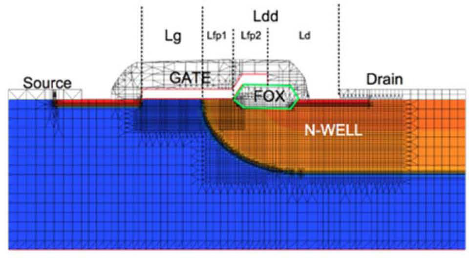
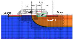
Figure 1 shows the basic cell structure of the HVMOS type N, over a P substrate, in which a N-WELL layer composes the drift region. The gate region, represented by Lg, must be large enough to avoid a punch-through. The correct selection of the Lg length allows the correct control of the current in the HVMOS.
In addition, the Ldd region, formed by Lfp1, Lfp2 and Ld, have to be optimized if a high BV and a low on resistance (Ron) want to be achieved [3]. Moreover, Ldd brings the capabilities to withstand high voltages.
Thus, using the Reduced Surface Field (RESURF) methodology one can achieve a tradeoff between the BV and the Ron [4]. Moreover, the field plate situated between the extensions of the gate terminal and the N-WELL layer must be considered, since it controls the conductivity of the HVMOS. When the HVMOS is in the OFF state, the field plate reduces the conductivity in the N-WELL layer due to a negative potential between the gate and the N-WELL. In the ON state a huge positive potential difference between the gate and the N-WELL appears and creates an accumulation area in the field-plate region, which allows forming a high conduction path from the drain to the source. In addition, during this state the Rdrift is slightly higher than the parasitic resistances of the drain and source terminals that are consequence of the metal interconnection. This fact is due to the N-WELL and the substrate impurity concentrations, which behave as a high resistance between the gate and drain terminals. In addition, Rdrift is an element that depends from the terminal bias voltages VGS and VDS, but since the dependency is much stronger with respect VGS, this voltage modulates the resistance of the channel of the HVMOS. Bias voltage VDS controls the electric field that drifts the inversion charge from the source to drain, which means that it limits the maximum current that the device can reach with a specific bias condition at the gate.
Prior to design the proposed HVMOS and due to the lack of a model for this kind of transistor, the doping profile has to be known. Since the doping profile is not public information, a procedure to estimate it was performed using the physical simulator ISE-TCAD from Synopsis, along with PSpice. The idea is to use the PSpice model of conventional CMOS FETs, provided by the foundry (MOSIS), and fit the DC l-V characteristics to approximate the circuit simulation results to the results from the physical simulator by means of variations of the doping profile. This procedure is summarized as follows:
- a)
Obtain by simulation the DC l-V characteristics of a NMOS transistor and a PMOS transistor in PSpice. This part is required for both transistors, due to the drift region in the HVMOS needs a N+ implant and this value is obtained from the doping profile of PMOS transistor.
- b)
In the ISE-TCAD simulator the transistors are built defining the active areas, gate, drain and source. Then by a manual tuning of the doping profile parameters, the DC l-V characteristics for both transistors are obtained and compared to the results from PSpice. It is worth to comment that the initial doping profile parameters were obtained from the previous work reported in [5], thus a minimum optimization process was required. In addition the depth of each layer was obtained from a confidential document under a Non-Disclosure Agreement with MOSIS.
Once the doping profile had been estimated, the design of the HVMOS was divided in two steps. The first step deals with the achievement of the maximum BV of the HVMOS (DC procedure), while the second step is related to the improvement of the extrinsic cutoff frequency (AC procedure).
2.1DC procedureOne of the variables of the structure in Figure 1 that plays an important role in the determination of the BV is Lg. A previous work in [5], experimentally evaluated several HVMOS with different Lg and concluded that with Lg less than 0.8 μm, the HVMOS presents a considerable leakage current in the drain and as a consequence, the gate cannot control the drain current of the transistor. It was also found that when the gate length is at least 1.2 μm (Lg =1.2 μm) the leakage current could be neglected. However, higher values of Lg result in a reduction of the cutoff frequency.
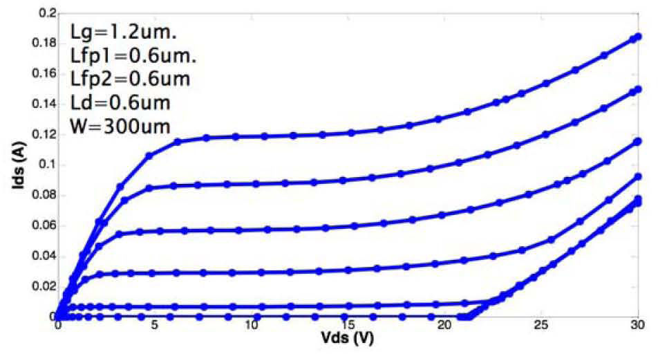
Several simulations in ISE-TCAD were performed using different values of Lg, Lfp1, Lfp2 and Ld. The simulation results and the experimental measurements reported in [5] suggest that with a Lg of 1.2 μm and Lfp1, Lfp2 and Ld equal to 0.6 μm, the HVMOS would reach a BV of 20 V as shown in Figure 2
It is worth to comment that the values were obtained by a manual tuning instead of an optimization procedure since ISE-TCAD is a physics simulator and an optimization routine will demand time consumption as well as computational resources that are not available in our facilities.
2.2AC procedurePads in CMOS FETs are parasitic elements, which contribute to degrade the gain and the cutoff frequency. In that sense, the pads have to be optimized to improve the performance of the HVMOS for RF applications.
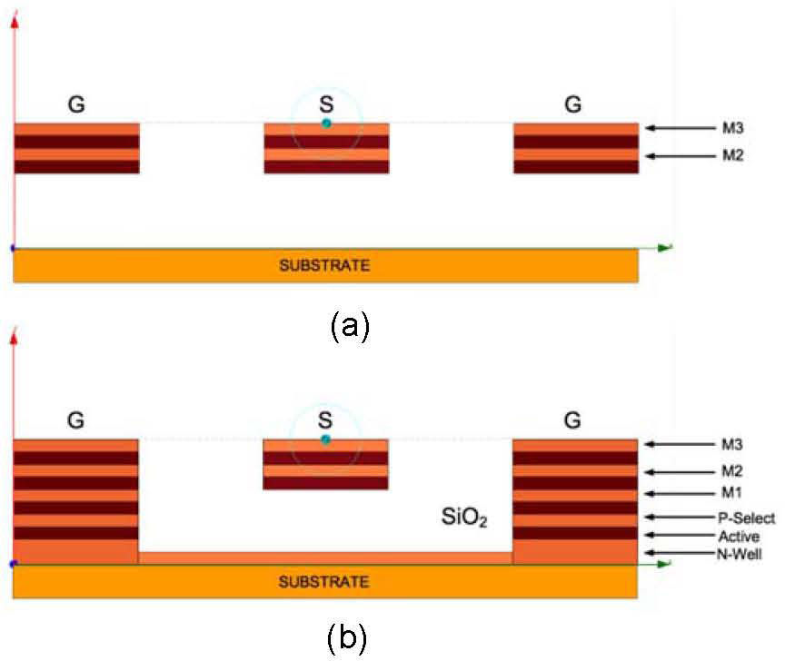
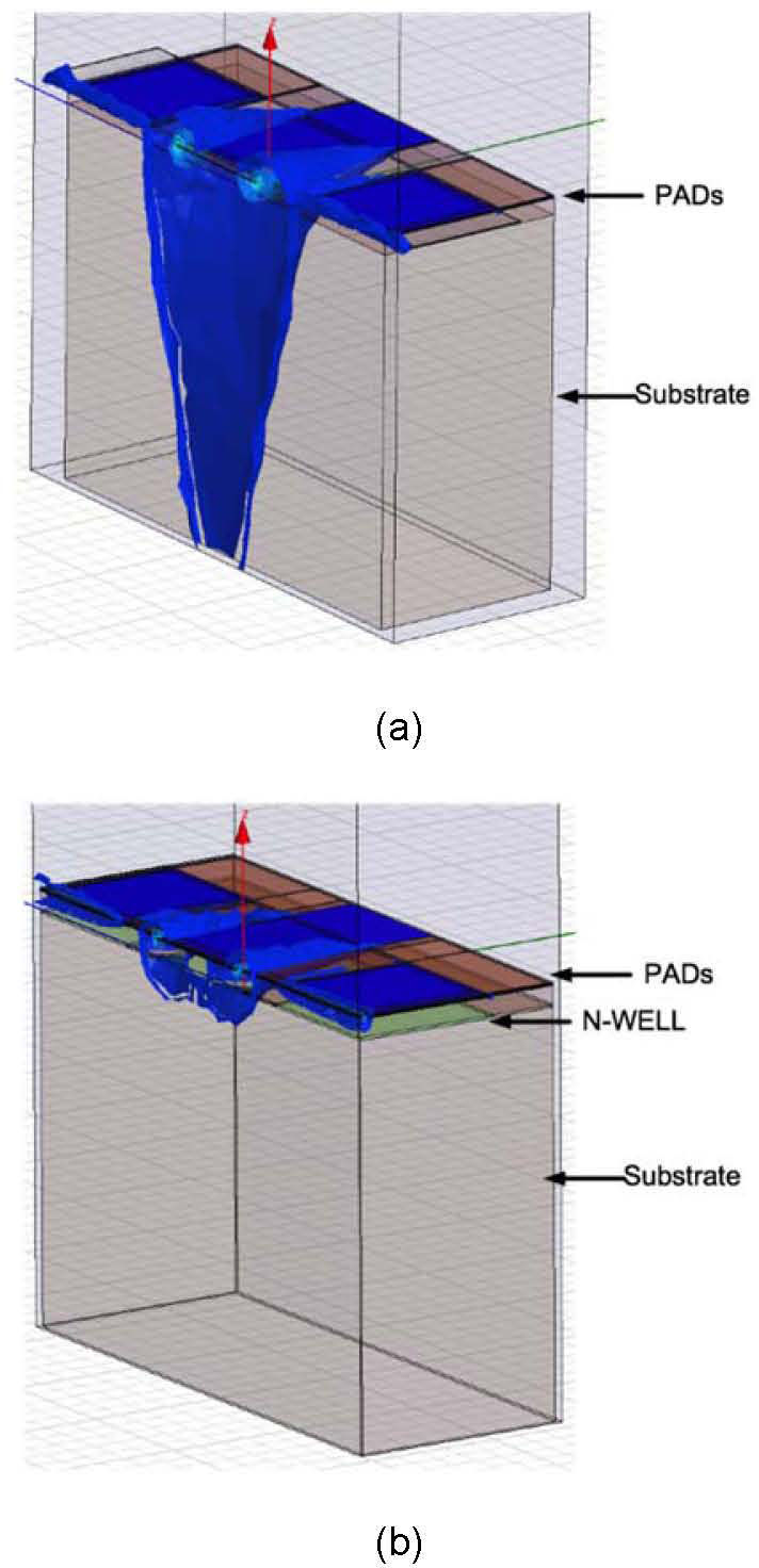
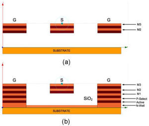
Figure 3.a shows the ground-signal-ground (GSG) pad structure available in the MOSIS fabrication process for an analog/digital application. In this standard structure the electric field goes down to the substrate, as shown in Figure 4.a, increasing the parasitic effects and producing a low cutoff frequency. To overcome this problem, some works propose to use the lower metallization layer as a shield to avoid couplings through the substrate [6]-[8].
It is worth to comment that the 0.5 μm technology available, in the Educational Program of MOSIS, has three metallization layers and is limited to use the technique mentioned above. Thus, a solution is to add a N-WELL layer to connect the ground terminals to a single point of reference, as depicted in Fig. 3.b. In this structure the signal pad is composed by two upper metallization layers, Figure 4.b shows the EM simulation of this structure, it can be seen how the electric field is isolated from the substrate by means of the N-WELL.
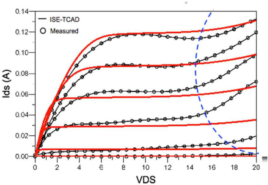
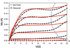
3Experimental ResultsFirst the l-V characteristic of the HVMOS was measured at wafer level using an AU4740 from Auriga Microwaves with a pulse width of 1000 us (see Figure 5). Notice that the measured l-V characteristics of the HVMOS have a similar behavior compared to the simulated l-V data done with ISE-TCAD. Also notice that the measured BVs do not correspond exactly to the data obtained from the physical simulator, this behavior can be attributed to the spreading of the lateral diffusion during the fabrication. This hypothesis is based on the fact that in the HVMOS FET the drift region is created by a NWELL layer of an approximately 3 μm of thickness. Thus, the lateral diffusion due to this layer is higher than the lateral diffusions of the drain and source, in consequence one should expect a decrease of Ron. Nevertheless this decrement is compensated with the RESURF method that was applied to reach a balance between the BV and Ron.
Finally, it is remarkable to mention that in our case the HVMOS does not posses two wells, this means that it is not possible to auto align the layers and the lateral diffusion parameter is always open to the fabrication process. This fact is not common in other technologies due that they require using two wells.
Another hypothesis that can explain the difference between the measured and simulated data is the uncertainty of the doping profile. Our efforts to determine the doping profile by means of a spectrometric study of the die, performed in the Centro de Investigación en Química Aplicada (CIQA), was not conclusive and unfortunately the doping profile was unable to be determined.
The measurements confirmed that the proposed design methodology results in a BV higher than the BV of conventional CMOS FETS, the latter being approximately of 7.0 V. The HVMOS achieved a maximum current of 120 mA that is very close to the value obtained in the simulation. The Ron was 0.27 mΩ/mm2, this value was computed at VDS = 0.1 V and VGS = 5.0 V for an effective area of 2.6 μm2. Moreover, the product (BV)2(Ron) that defines a power figure of merit indicates a value of 1.48 MW/mm2. In addition, the current level can be increased modifying the gate width of the transistor and reducing the breakdown voltage can decrease the value of Ron.
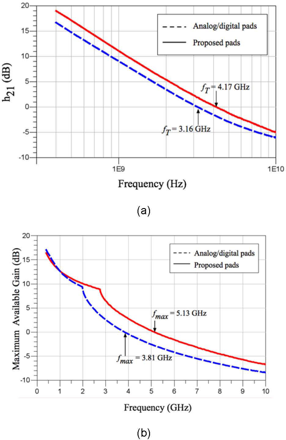
Regarding to the RF performance, a PNA-X N5242A was used to measure the HVMOS. As mentioned before the classical digital/analog pad technology precludes the increase of the extrinsic fT in standard MOS transistors. This fact can be verified in Figure 6.a and 6.b, in which the extrinsic fT and fmax of the HVMOS with analog/digital pads is compared with the response of a HVMOS with the proposed pads. Both HVMOS were biased as a class A power amplifier (VDS = 9.5 V and VGS = 2.5 V). It is observed an improvement of 31.9% and 34.7% of the fT and fmax respectively.
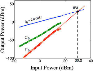
Moreover, IP3 of +30.2 dBm was achieved with the proposed HVMOS, which represents a high linear transistor, as shown in Figure 7. In this case the HVMOS was biased at the maximum transconductance point (VDS = 6.8 V and VGS = 3.4 V).
4ConclusionsThis paper presents a methodology to design HVMOS devices in standard bulk CMOS 0.5 μm technology. To validate the proposed new structure several HVMOS were fabricated. It was shown that modifying the lengths that compose the drift region could increase the breakdown voltage. Once the optimum lengths are determined, the next step is to design a suitable CMOS PAD that allows the device to operate at higher frequencies. Experimental results from a CMOS FET built with the structure proposed in this work demonstrated the achievement of 20 V of breakdown voltage. In addition, the proposed CMOS pads demonstrated an enhancement of 31.9% and 34.7% in fT and fmax, respectively, in comparison to analog/digital pads. These improvements will allow using MOS technology in medium power RF applications.


